
Production method for nano focusing X ray lens combination
A combined lens and nano-focusing technology, which is applied in the field of X-ray microstructured optical devices, can solve the problems of poor light-gathering ability, high roughness, and low X-ray radiation transmittance of the combined lens, so as to improve the radiation transmittance, The light-gathering ability is improved, and the effect of increasing the light-gathering aperture
Patent Information
- Authority / Receiving Office
- CN · China
- Patent Type
- Patents(China)
- Current Assignee / Owner
- Publication Date
- 2010-12-08
- Estimated Expiration
- Not applicable · inactive patent
Smart Images
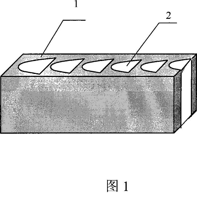
Figure 1 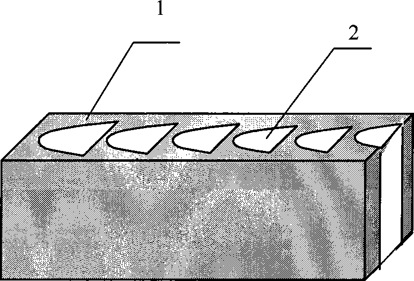
Figure 2
Abstract
Description
(1) Technical field
[0001] The invention relates to an X-ray microstructure optical device, in particular to a manufacturing process of a microstructure X-ray optical device capable of focusing X-rays at a nanoscale, and is suitable for the production of one-dimensional nano-focus X-ray combined lenses made of silicon materials. (2) Background technology
[0002] X-ray composite lens is an X-ray microstructure optical device based on refraction effect proposed by A. Snigirev in 1996, which is suitable for high-energy X-ray band (that is, X-ray radiation energy exceeds 5keV). It has the advantages of no need to bend the optical path, good high temperature stability and easy cooling, simple and compact structure, and low requirements on the surface roughness of the lens. It has broad application prospects in the field of ultra-high resolution X-ray diagnostic science and technology. In recent years, research on various X-ray diagnostic techniques based on X-ray combined lense...
Examples
Embodiment 1
[0024] Refer to attached figure 1 , a method of manufacturing a silicon material one-dimensional nano-focus X-ray composite lens, the steps are as follows:
[0025] (A) use electron beam etching technology to make a photolithographic mask plate of glass substrate metal chromium material, the photolithographic mask pattern is composed of a plurality of combined lens refraction units coaxially arranged in sequence, and the refraction unit is composed of The through-hole-shaped air gap is formed together with the lens main body material. The cross-sectional shape of the air gap is elliptical, and the maximum diameter of the air gap corresponding to the minor axis of the ellipse is smaller than the minor axis of the ellipse. The elliptical air gap of the lens unit The long axis of the gap is on the same straight line, and the size of the ellipse corresponding to the air gap gradually decreases, and they are arranged in order from large to small;
[0026] (B) Carry out conventiona...
Embodiment 2
[0034] In the technical scheme of the present embodiment, the thickness of the ultraviolet negative photoresist in the step (C) is 1 micron, and the thickness of the aluminum metal film described in the step (E) is 150 nanometers, and the total depth in the step (G) The etching time of silicon is 30 minutes, the etching phase lasts 6 seconds, the gas SF 6 Injection rate 130 sccm, working pressure 2.4 Pa, working power 600 watts, deposition phase duration 5 seconds, gas C 4 f 8 The injection rate is 120sccm, the working pressure is 1.9 Pa, and the working power is 600 watts, and the rest are the same as in Example 1.
Embodiment 3
[0036] In the technical scheme of the present embodiment, the thickness of the ultraviolet negative photoresist in the step (C) is 3 microns, and the thickness of the aluminum metal film described in the step (E) is 200 nanometers, and the total depth in the step (G) The etching time of silicon is 40 minutes, the duration of etching phase is 6.5 seconds, the gas SF 6 The injection rate is 135 sccm, the working pressure is 2.5 Pa, the working power is 610 W, the duration of the deposition phase is 5.5 seconds, and the gas C 4 f 8 The injection rate is 125 sccm, the working pressure is 2.0 Pa, and the working power is 610 watts, and the rest are the same as in Example 1.