
Production for aluminium-material X-ray assembled lens
A technology for combining lenses and manufacturing methods, which is applied in the directions of lenses, radiation/particle processing, photolithographic process exposure devices, etc., can solve the problems of large absorption of X-ray radiation, large spherical aberration, etc., and achieves increased light collection aperture and small material restrictions. , The effect of easy beam alignment
Patent Information
- Authority / Receiving Office
- CN · China
- Patent Type
- Patents(China)
- Current Assignee / Owner
- Publication Date
- 2006-11-22
- Estimated Expiration
- Not applicable · inactive patent
Smart Images
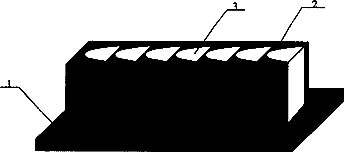
Figure 1
Abstract
Description
(1) Technical field
[0001] The invention relates to an X-ray microstructure optical device, in particular to a manufacturing process of an X-ray combined lens, which is suitable for the production of an aluminum material parabolic X-ray combined lens. (2) Background technology
[0002] X-ray combined lens is a new type of X-ray microstructure optical element suitable for high-energy X-ray band (that is, X-ray radiation energy exceeding 5keV) proposed by A. Snigirev in 1996. The X-ray combination lens has many advantages, such as no need to bend the optical path, good high temperature stability and easy cooling, simple and compact structure, and low requirements on the surface roughness of the lens. In particular, it is suitable for occasions where the energy of X-ray radiation exceeds 5keV, so the element has broad application prospects in scientific and technical research. In recent years, research on various X-ray diagnostic techniques based on X-ray combined lenses is ve...
Examples
Embodiment 1
[0029] Refer to attached figure 1 , a kind of manufacture method of aluminum material parabolic X-ray compound lens, comprises the preparation of X-ray lithography mask, the preparation of X-ray lithography substrate and the formation of final aluminum material lens; (1) X-ray lithography mask The preparation includes the following steps:
[0030] (A) Spin-coating a layer of polyimide coating on the surface of the silicon substrate through conventional cleaning treatment, baking and curing;
[0031] (B) growing an electroformed cathode film of a copper material on the surface of the solidified sample sheet;
[0032] (C) Coating a layer of AZP4000 photoresist on the surface of the electroformed cathode film, carrying out photoetching, development, and hardening of the above photoresist to form a photoresist pattern structure;
[0033] (D) growing one deck metal thin film on photoresist pattern structure, described metal thin film material is gold, and its thickness is less th...
Embodiment 2
[0045] In the technical scheme of the present embodiment, the metal material electroforming cathode film described in the step (B) is a titanium material, and the thickness of the PMMA coating on the surface of the titanium sheet is 1000 microns in the step (1), and all the other steps are the same as in Example 1.
Embodiment 3
[0047] In the technical scheme of the present embodiment, the metal material electroforming cathode film described in the step (B) is a nickel material, and the thickness of the PMMA coating on the surface of the titanium sheet is 2000 microns in the step (1), and all the other steps are the same as in Example 1.
[0048] Process tests have been carried out on the above three embodiments, and it can be seen from the test results that they all meet the requirements of the structural shape and size of the X-ray combined lens, and the process test effect of embodiment 2 is the best.