
Process for mfg. one-dimensional X ray refracted diffraction micro structural component of polymethyl methyl acrylate material
A technology of polymethyl methacrylate and its production method, which is applied in X-ray/γ-ray/particle irradiation therapy, material analysis, material analysis using wave/particle radiation, etc. It can solve the problem of low device structure depth and surface roughness Low, large structure depth and other issues, to achieve the effect of small material restrictions, good focal spot quality, and reduced X-ray absorption
Patent Information
- Authority / Receiving Office
- CN · China
- Patent Type
- Patents(China)
- Current Assignee / Owner
- Publication Date
- 2007-07-18
- Estimated Expiration
- Not applicable · inactive patent
Smart Images
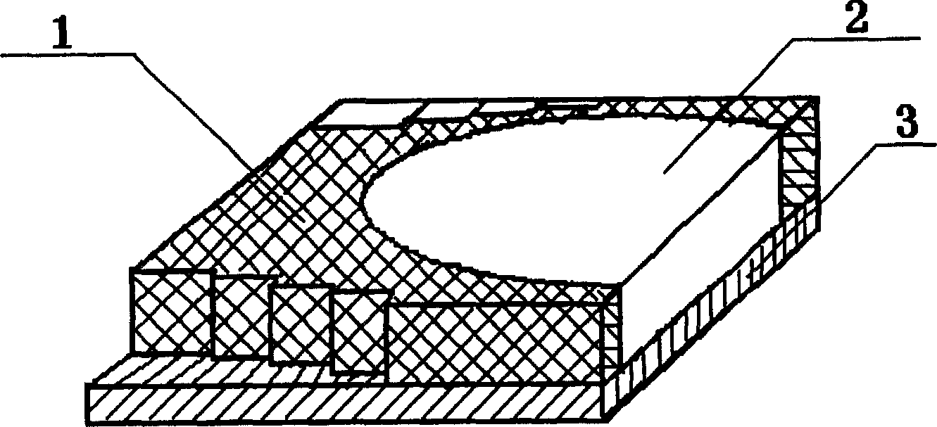
Figure 1
Abstract
Description
(1) Technical field
[0001] The invention relates to an X-ray microstructure optical device, in particular to a manufacturing process of a microstructure X-ray optical device based on the dual effects of refraction and diffraction, and is suitable for polymethyl methacrylate organic material one-dimensional X-ray refractive diffraction microstructure device Production occasion. (2) Technical background
[0002] The X-ray combination lens is a kind of X-ray microstructure optical device based on refraction effect, which is suitable for high-energy X-ray wave band (that is, the X-ray radiation energy exceeds 5keV) proposed by A. Snigirev in 1996. It has the advantages of no need to deflect the light path, good high temperature stability and easy cooling, simple and compact structure, and low requirements on the surface roughness of the lens. It has broad application prospects in the field of ultra-high resolution X-ray diagnostic science and technology. In recent years, research on ...
Examples
Embodiment 1
[0029] 1, a method for manufacturing a one-dimensional X-ray diffraction microstructure device of polymethyl methacrylate material, the one-dimensional X-ray diffraction microstructure device includes a plurality of lens units arranged coaxially in sequence The lens unit is composed of a lens body with an air gap, and the upper side wall of the lens body is provided with upward stepped steps, and the step width of each step is equal; the lower side wall of the lens body is opened There are downward stepped steps arranged symmetrically with the steps of the upper side wall of the lens with the axis as the center line, the lens body is provided with an open air gap, the cross-sectional shape of the air gap is semi-elliptical, and the air gap The maximum aperture size corresponding to the minor axis of the ellipse is smaller than the minor axis of the ellipse, the major axis of the elliptical air gap of the lens unit is located on the same straight line, and the manufacturing method ...
Embodiment 2
[0044] In the technical solution of this embodiment, the thickness of the polyimide material in step (C) is 5 microns, the metal material electroformed cathode film in step (D) is titanium material, and the surface of the titanium sheet is coated in step (K) The thickness of the coated polymethyl methacrylate is 500 microns, and the rest of the steps are the same as in Example 1.
Embodiment 3
[0046] In the technical scheme of this embodiment, the metal material electroformed cathode film described in step (D) is titanium material with a thickness of 400 nanometers, and in step (K), the thickness of the polymethyl methacrylate coated on the surface of the titanium sheet is 800 Micron, the remaining steps are the same as in Example 1.