
Method of making X-ray combination lenses
A technology for combining lenses and manufacturing methods, which is applied in the fields of lenses, radiation/particle processing, optics, etc., can solve the problems of difficult manufacturing process, poor safety, low yield, etc., and is conducive to batch manufacturing and integration, and has high processing accuracy. , the effect of cost reduction
Patent Information
- Authority / Receiving Office
- CN · China
- Patent Type
- Patents(China)
- Current Assignee / Owner
- Publication Date
- 2006-11-15
- Estimated Expiration
- Not applicable · inactive patent
Smart Images
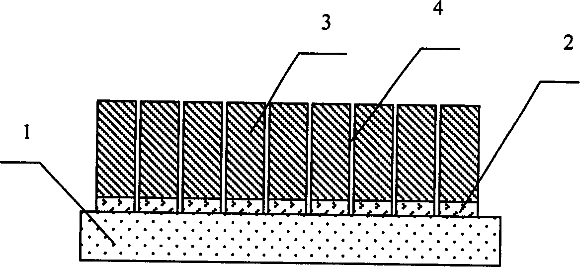
Figure 1 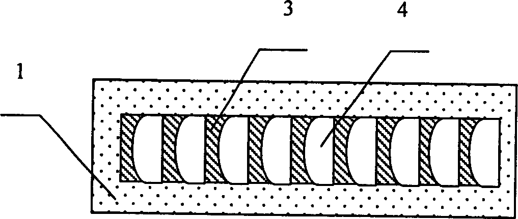
Figure 2
Abstract
Description
(1) Technical field
[0001] The invention relates to an X-ray microstructure optical device, in particular to a manufacturing process of an X-ray combined lens, which is suitable for the occasion of making the X-ray combined lens. (2) Background technology
[0002] Creating an X-ray lens was long considered impossible because all materials refract too weakly and absorb too strongly at X-ray wavelengths. In order to realize the focusing of X-ray beams, scientists have successively developed grazing incidence X-ray total reflection mirrors, transmission X-ray zone plates, multilayer films, crystal X-ray Bragg-Fresnel elements and X-ray catheter elements, etc. However, these components are difficult to use in the range of X-ray radiation energy higher than 5keV. In 1996, Snigirev reported an X-ray combination lens that can be used in the high-energy X-ray band. The combined lens has many advantages, such as no need to bend the optical path, good high temperature stability and ...
Examples
Embodiment 1
[0022] refer to figure 1 , figure 2 , a method for making an X-ray composite lens, comprising the steps of: (A) growing a layer of electroformed cathode film (2) by sputtering or evaporation on a silicon or glass substrate (1) that has been conventionally cleaned, The film (2) is a copper material, where the copper material can be replaced by titanium or nickel or gold or titanium oxide material;
[0023] (B) Coating the first layer of AZP4903 positive photoresist on the electroformed cathode film (2) at a low speed, and baking and curing with a hot plate, the baking temperature is 97.5°C, and the baking time is 8 minutes;
[0024] (C) On the cured first layer of AZP4903 positive photoresist, coat the second layer of AZP4903 positive photoresist at a low speed, and bake and cure with a hot plate, the baking temperature is 90 ° C, and the baking time is 20 minutes;
[0025] (D) carry out photoetching to AZP4903 photoresist with ultraviolet lithography method, and its photoe...
Embodiment 2
[0032] In the technical solution of this embodiment, the electroformed cathode film (2) is titanium material in step (A); in step (B), the baking temperature is 102.5° C., and the baking time is 8 minutes, and the remaining steps are exactly the same as in Example 1. Same.
Embodiment 3
[0034] In the technical solution of this embodiment, the electroformed cathode film (2) is made of nickel material in step (A); in step (B), the baking temperature is 102.5° C., and the baking time is 12 minutes, and the remaining steps are completely the same as in Example 1. Same.