
Reflection-permeation array substrate and method for manufacturing same
A manufacturing method and technology for an array substrate, which are applied in the photoengraving process, optics, optomechanical equipment and other directions of the pattern surface, can solve the problems of difficult setting and rising manufacturing costs, and achieve the goal of reducing the problem of rising costs, improving quality, The effect of simplifying manufacturing engineering
Patent Information
- Authority / Receiving Office
- CN · China
- Patent Type
- Patents(China)
- Current Assignee / Owner
- Publication Date
- 2010-09-08
Smart Images
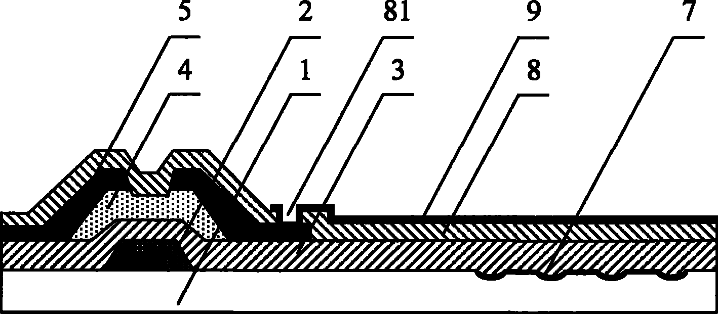
Figure 1 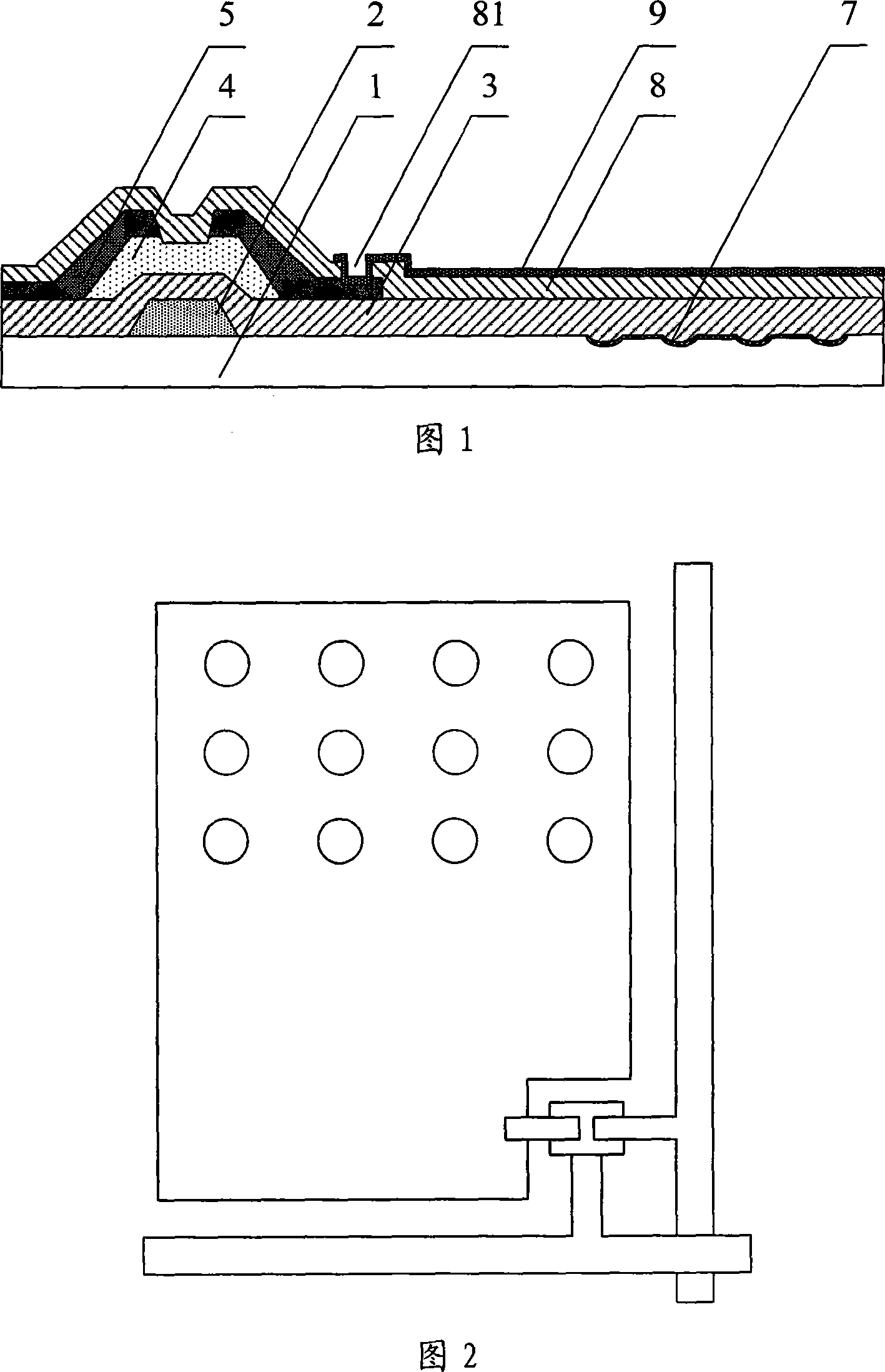
Figure 2 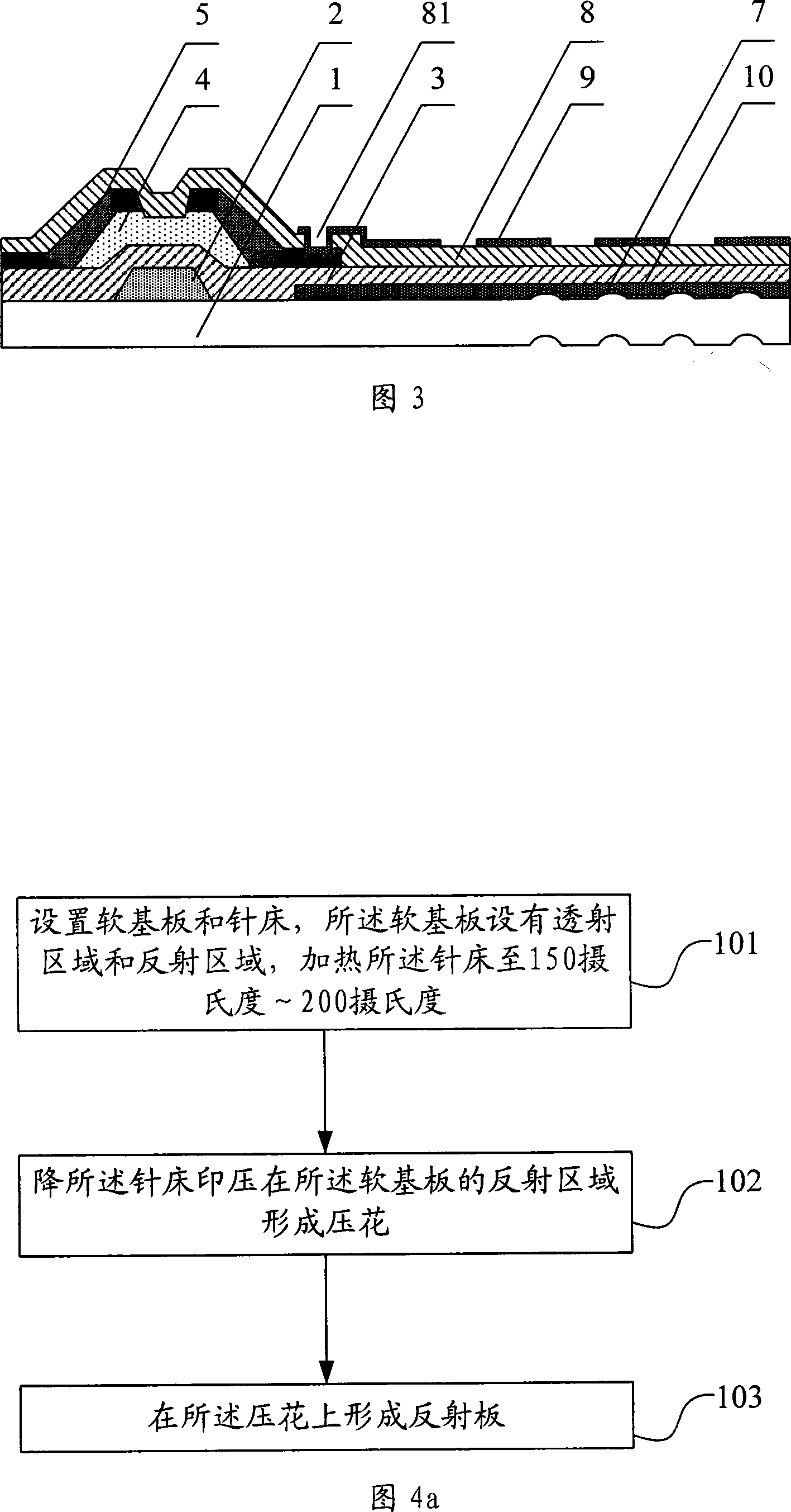
Figure 3
Abstract
Description
technical field
[0001] The present invention relates to an array substrate and a manufacturing method thereof, in particular to an anti-transmission array substrate and a manufacturing method thereof. Background technique
[0002] The liquid crystal display device is one of the most used flat panel display devices at present. It is mainly composed of two substrate structures and a liquid crystal layer injected between the substrate structures. The two substrate structures are provided with electrodes that can generate an electric field, and the electrodes generate a voltage. The liquid crystal molecules in the rear liquid crystal layer move with the electric field, and the liquid crystal molecules rotate in a certain direction under the action of the electric field, so that light passes through the liquid crystal layer according to a certain refractive index.
[0003] Liquid crystal display devices can be classified into transmissive type, anti-transmissive type and reflecti...
Examples
no. 1 example
[0034]FIG. 1 is a schematic structural diagram of a first embodiment of a transflective array substrate of the present invention. As shown in Figure 1, the anti-transmissive array substrate includes: a soft substrate 1 and an array body, wherein the soft substrate 1 is provided with a transmissive area and a reflective area, and embossing is formed on the soft substrate 1 corresponding to the reflective area. The flower is composed of pits, and a reflective plate 7 with uniform thickness is arranged on the embossing. The main body of the array is located on the side of the soft substrate 1 provided with the reflective plate 7. The main body of the array includes grid lines (not shown in the figure), grid electrodes 2 , gate insulating layer 3, active layer 4, source and drain electrodes 5, data lines (not shown in the figure), passivation layer 8 and pixel electrode 9; the main structure of the array is specifically: a soft substrate provided with a reflector 7 1 is provided w...