
Lateral diffused metal oxide semiconductor transistor structure capable of avoiding double-hump effect
An oxide semiconductor and transistor technology, applied in semiconductor devices, electrical components, circuits, etc., can solve the problems of transistor leakage, low turn-on voltage, low turn-on voltage, etc., and achieve the effect of constant threshold voltage Vt and uniform thickness
Patent Information
- Authority / Receiving Office
- CN · China
- Current Assignee / Owner
- Publication Date
- 2010-06-02
Smart Images
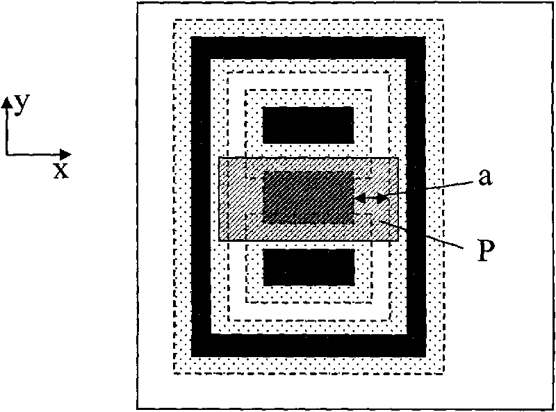
Figure 1 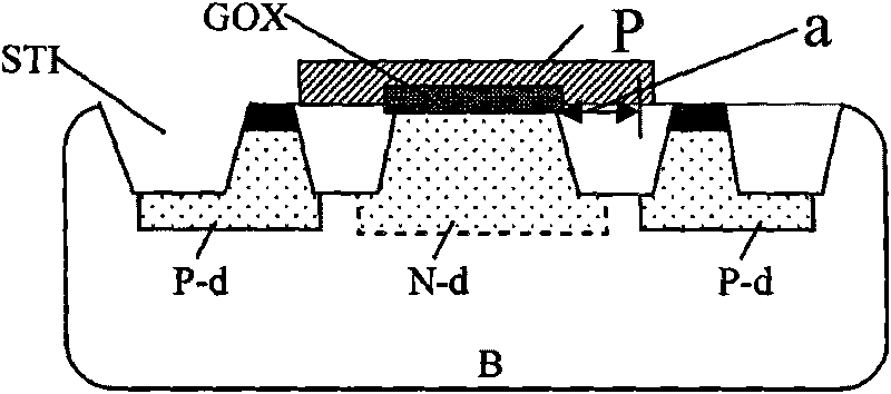
Figure 2 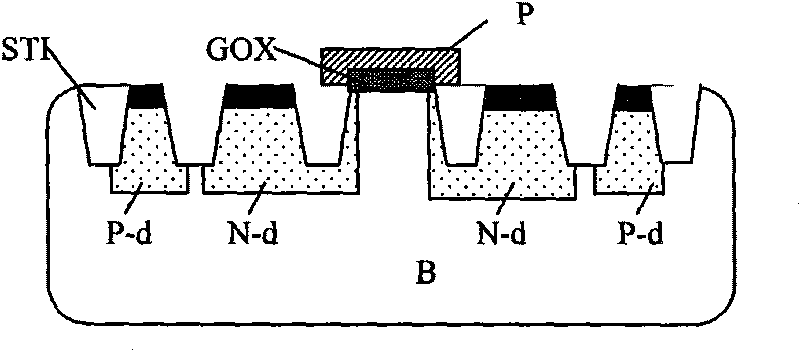
Figure 3
Abstract
Description
technical field
[0001] The invention relates to a structure of a laterally diffused metal oxide semiconductor transistor, and further relates to a structure of a laterally diffused metal oxide semiconductor transistor which avoids the double peak effect. Background technique
[0002] Laterally Diffused N type Metal Oxidesemiconductor (LDNMOS) plays an important role in the design and manufacture of several circuits. For example, a laterally diffused metal oxide semiconductor transistor (HV LDNMOS) is widely used in a driver chip of a thin film transistor liquid crystal display.
[0003] The structure diagram of the current LDNMOS is as follows figure 1 and figure 2 as shown, figure 1 is a schematic top view of a known LDNMOS structure; figure 2 for figure 1 Schematic diagram of the cross-section of the LDNMOS along the x direction; image 3 for figure 1 Schematic diagram of the cross-section of the LDNMOS along the y direction. The LDNMOS includes a base layer B, a...
Examples
Embodiment Construction
[0021] In order to better understand the technical content of the present invention, specific embodiments are given together with the attached drawings for description as follows.
[0022] Figure 4 It is a schematic top view of the LDNMOS structure disclosed in the present invention; Figure 5 for Figure 4 Schematic cross-sectional view of the LDNMOS structure along the x direction; Figure 6 for Figure 4 A schematic cross-sectional view of the LDNMOS structure along the y direction.
[0023] Please also refer to Figure 4~6 In this embodiment, the LDNMOS structure includes a base layer B, an oxide layer GOX, and a polysilicon layer P in order from bottom to top.
[0024] In this embodiment, the base layer B is an N well, and the polysilicon layer P formed thereon serves as the gate G of the LDNMOS. On both sides of the oxide layer GOX in the base layer B, there are corresponding N-type drift regions N-d as the source S and drain D of the LDNMOS.
[0025] The N-type ...