
Manufacturing method of high-density interconnected printed circuit board
A printed circuit board and high-density interconnection technology, which is applied in the secondary processing of printed circuits, the formation of electrical connections of printed components, and the application of non-metallic protective layers, etc., can solve the problems of poor efficiency and good product rate, increased production management hours, and Pollution control costs and other issues to achieve the effect of avoiding poor conduction, improving yield, and high yield
Patent Information
- Authority / Receiving Office
- CN · China
- Patent Type
- Applications(China)
- Current Assignee / Owner
- Publication Date
- 2012-07-18
Smart Images
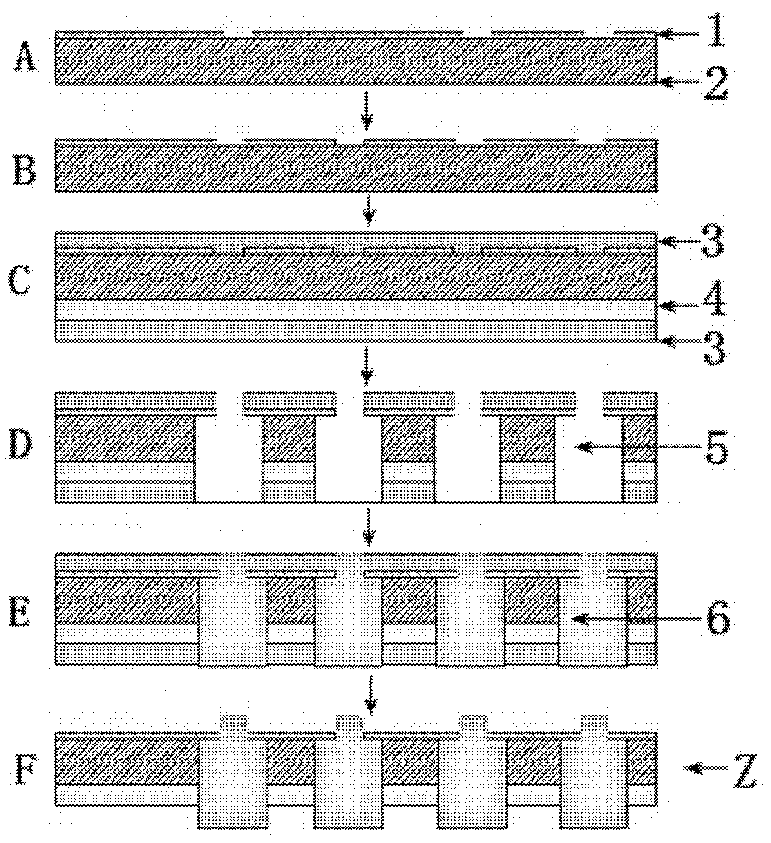
Figure 1 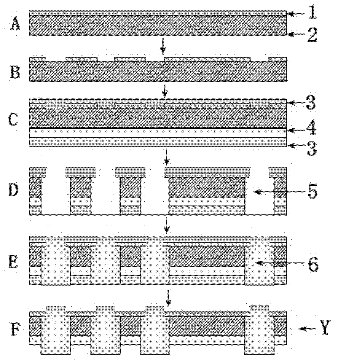
Figure 2 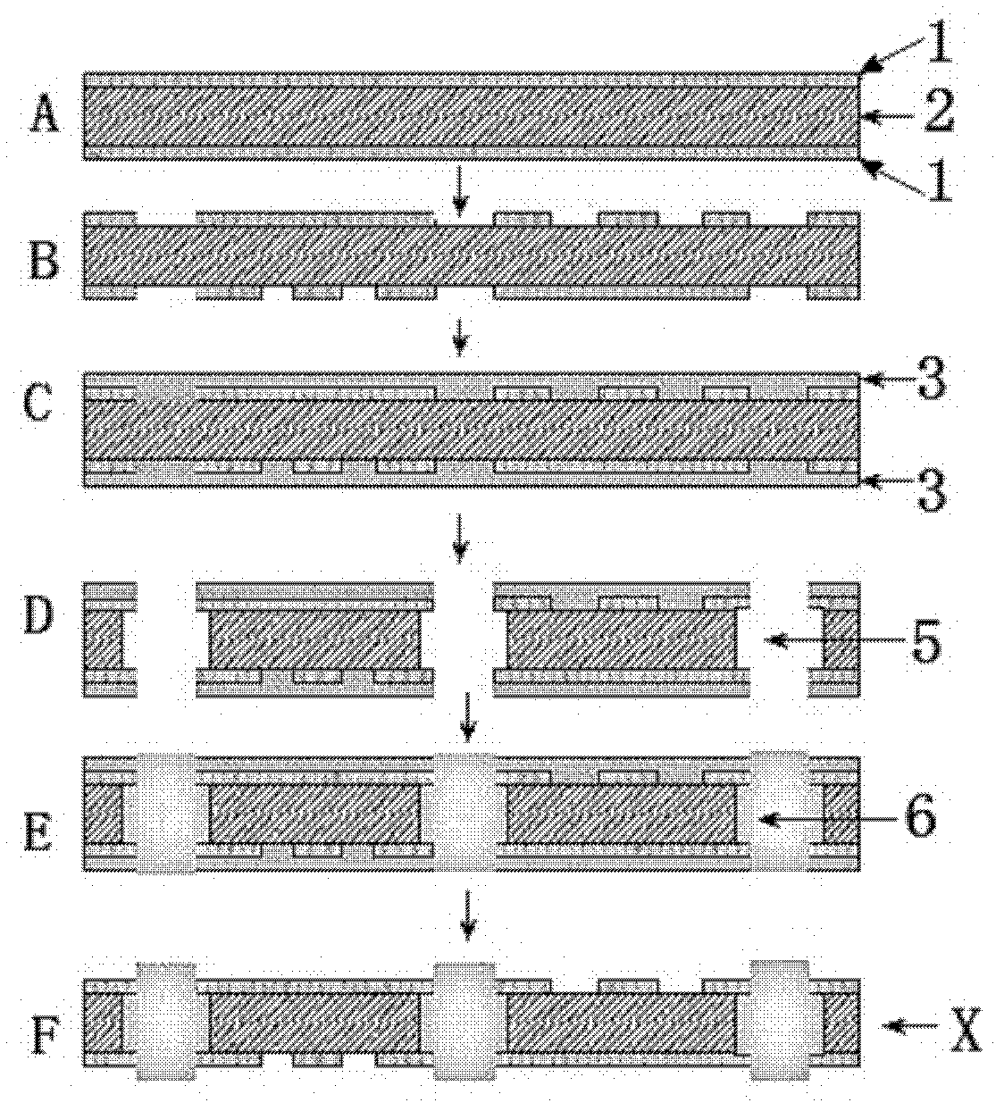
Figure 3
Abstract
Description
technical field
[0001] The invention belongs to the field of printed circuit boards, and mainly relates to a method for manufacturing high-density interconnected printed circuit boards. Background technique
[0002] The traditional multi-layer board is formed by alternately laminating and hot-pressing multiple substrates and adhesive material layers formed with circuits, and then using the drilling and metallization process in the holes to achieve the connection and conduction function between the circuits of each layer. . Under the premise that electronic products tend to be multi-functional and complex, the contact distance of integrated circuit components will be reduced, and the speed of signal transmission will be relatively increased, followed by an increase in the number of connections and the length of wiring between points. Local shortening, these require the application of high-density circuit configuration and microvia technology to achieve the goal. However, du...
Examples
Embodiment
[0029] Embodiment: A method for manufacturing a high-density interconnected printed circuit board. The high-density interconnected printed circuit board consists of a core structure X located in the middle, several intermediate structures Y located on both sides of the core structure, and an outermost The outer structure Z is superimposed and heat-pressed, such as Figure 4 shown;
[0030] Wherein, the preparation method of the outer layer structure Z is as follows: figure 1 As shown in A-F, the copper foil layer 1 of the single-sided copper foil substrate composed of the copper foil layer 1 and the insulating layer 2 is windowed, and then a layer of protective film 3 is pressed on the surface of the copper foil layer 1 and at the same time A layer of adhesive film 4 and a layer of protective film 3 are pressed on the surface of the insulating layer 2. The protective film 3 is located outside the adhesive film 4. A through hole 5 is drilled on the single-sided copper foil sub...