
Electroplating tank
A technology of electroplating tank and electroplating solution, which is applied in the direction of plating tanks, circuits, electrical components, etc., can solve the problems of difficult control of uniformity, and achieve the effects of consistent surface loss, extended length, and reduced quantity
Patent Information
- Authority / Receiving Office
- CN · China
- Patent Type
- Patents(China)
- Current Assignee / Owner
- Publication Date
- 2016-08-17
Smart Images
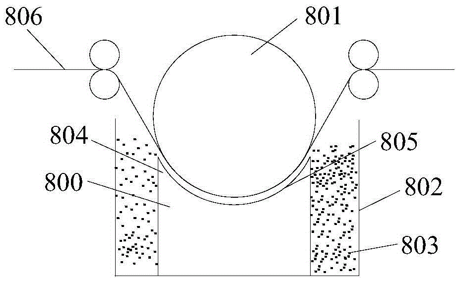
Figure 1 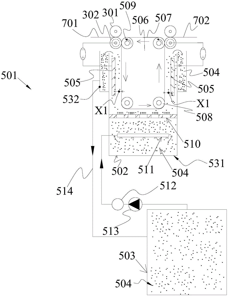
Figure 2 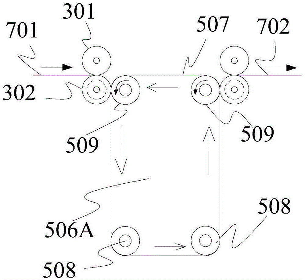
Figure 3
Abstract
Description
technical field
[0001] The invention belongs to the technical field of manufacturing solar cell equipment, in particular to a roll-to-roll electroplating tank. Background technique
[0002] CIGS (copper indium gallium selenide) thin film solar cells have excellent light absorption constant, only need 1.5 micron ultra-thin absorption layer, stable photoelectric conversion efficiency, wide spectral response range, adjustable energy band, strong radiation resistance, no light It has the advantages of light-induced gain, low-light gain, light weight, low cost, and easy installation, which have become the focus of research in the field of solar energy. Its typical structure is: metal back electrode Mo layer, CIGS absorption layer, buffer layer CdS, window layer high resistance i:ZnO, low resistance ZnO:Al, MgF2 anti-reflection film and Ni-Al gate electrode.
[0003] The CIGS absorbing layer is composed of four elements: Cu, In, Ga, and Se. The photoelectric conversion efficiency...
Examples
Embodiment Construction
[0073] In order to make the object, technical solution and advantages of the present invention clearer, the present invention will be further described in detail below in conjunction with the accompanying drawings and embodiments. It should be understood that the specific embodiments described here are only used to explain the present invention, not to limit the present invention.
[0074] The implementation of the present invention will be described in detail below in conjunction with specific drawings.
[0075] Such as Figure 2-4a Shown is the preferred embodiment provided by the present invention.
[0076] An electroplating tank provided in this embodiment is a working tank where electroplating occurs, and is used to deposit copper or gallium or indium or selenium on a surface of a substrate. It can be understood that the substrate is conducive to depositing copper or gallium or The indium or selenium element absorbing layer is made of conductive material, such as alumin...