

A storage system and a reading and writing method using the storage system
A storage system and file system technology, applied in the storage field, can solve the problems of data damage to the entire file system, increase the cost of solid-state hard disks, and MRAM is expensive, and achieve the effect of improving performance, ensuring read operation performance, and ensuring write operation performance.
Patent Information
- Authority / Receiving Office
- CN · China
- Patent Type
- Patents(China)
- Current Assignee / Owner
- Publication Date
- 2018-09-14
Smart Images
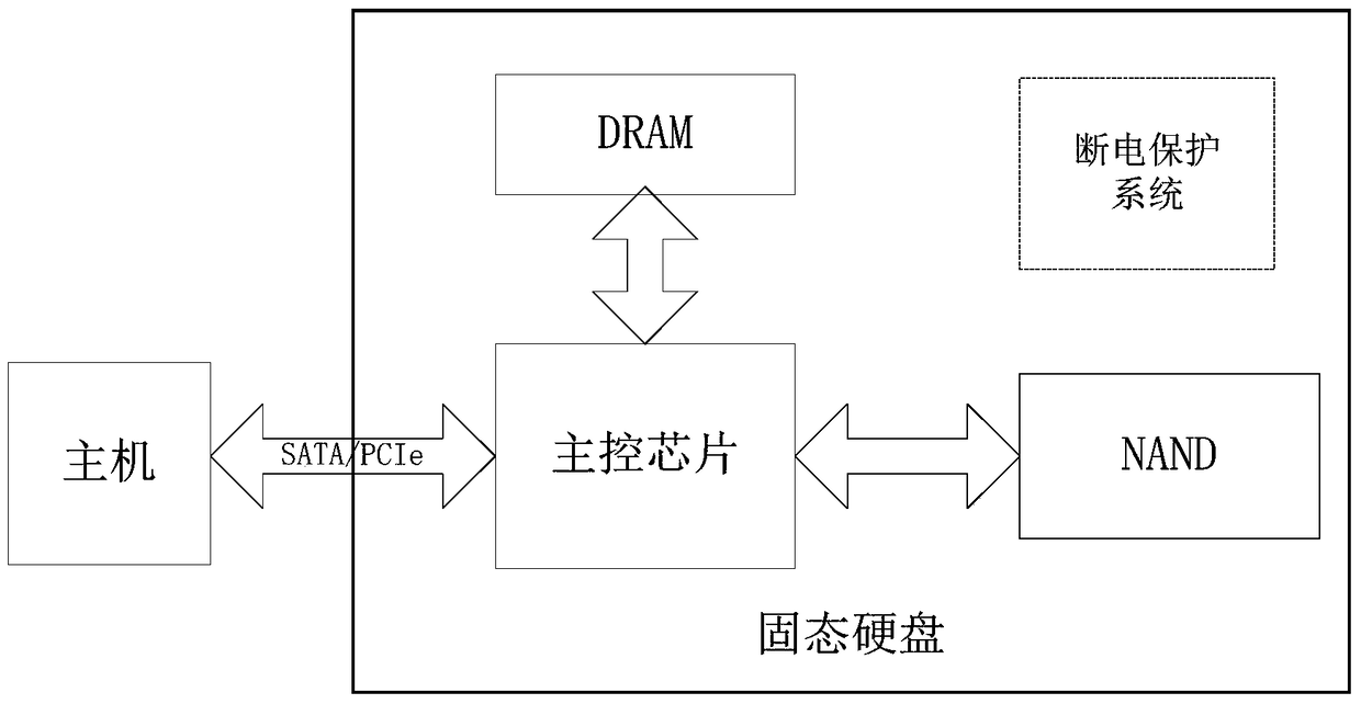
Figure 1 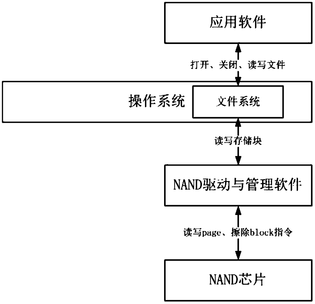
Figure 2 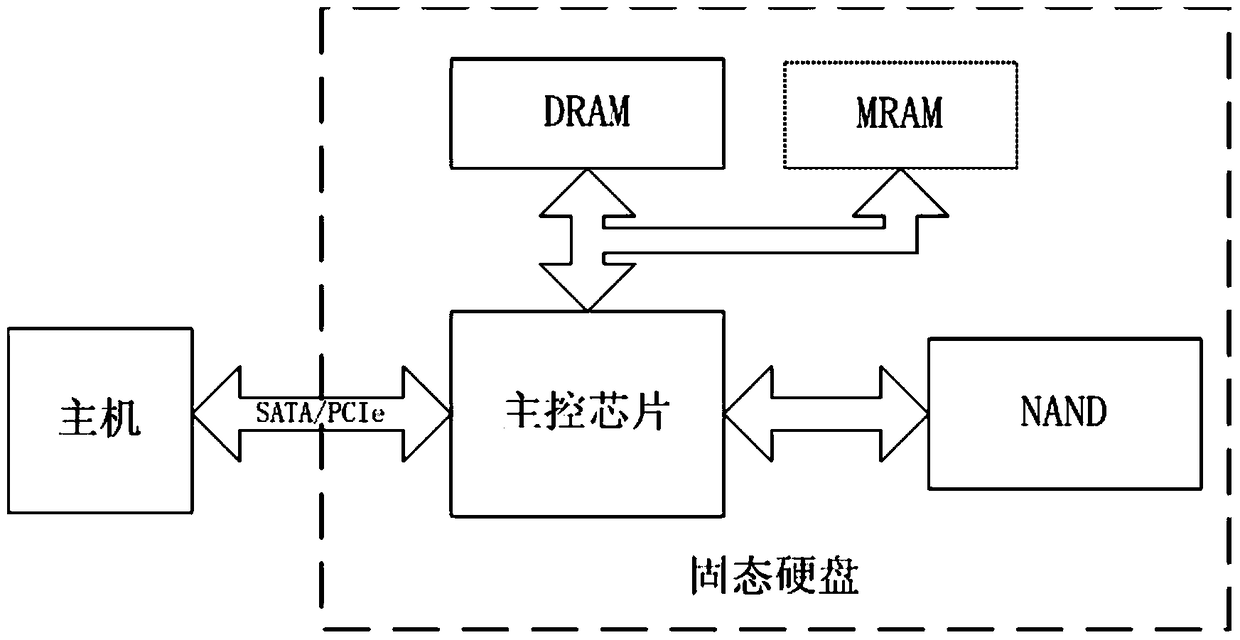
Figure 3
Abstract
Description
technical field
[0001] The invention relates to the field of storage technology, in particular to a storage system and a reading and writing method using the storage system. Background technique
[0002] Currently, the development of NAND flash memory technology has promoted the SSD industry. Such as figure 1 As shown, high-speed serial interfaces such as SATA, PICe and other technologies are used between the SSD and the host. The interior consists of a set of NAND chips for storing data, DDR DRAM (memory) for supporting calculation and caching data, and a main control chip (SSD Controller). Sometimes a power failure protection system is also required.
[0003] NAND is a storage device that reads and writes as a whole. The smallest readable unit is called a page, and the smallest erasable unit is called a block. A block is often composed of many pages. After the block is erased, the pages inside can be written separately Enter operation. Write operations are slow, much ...
Examples
Embodiment Construction
[0062] Such as Figure 4 As shown, the storage system of an embodiment of the present invention includes a host memory and a solid-state hard disk. The solid-state hard disk includes a main control chip, a NAND chip, and MRAM. Includes write cache.
[0063] The MRAM is connected to the main control chip of the solid-state hard disk through the DDR DRAM interface.
[0064] The logical address and physical address comparison table is stored in the NAND chip, which is read from the NAND to the host memory by the file system when the computer is turned on. Using this scheme, since the entire logical address and physical address comparison table is read into the host memory, random read and write performance will not be sacrificed, but a large amount of memory in the host will be consumed, so this scheme is more suitable for servers.
[0065] The logical address and physical address mapping table is written back to NAND by the file system when the computer is turned off or the ho...