
A kind of thick copper board of different types of circuit boards and the manufacturing method of circuit boards
A production method and technology of thick copper plate, applied in the direction of multi-layer circuit manufacturing, printed circuit manufacturing, circuit lamination, etc., can solve the problem that the expansion and shrinkage of copper plate and FR4 substrate is not easy to control, and it is impossible to arrange and combine multiple circuit boards. , increase production costs and other issues, to achieve the effect of reducing production process and production time, avoiding sheet material expansion and shrinkage, and saving production costs
Patent Information
- Authority / Receiving Office
- CN · China
- Patent Type
- Patents(China)
- Current Assignee / Owner
- Publication Date
- 2019-02-22
Smart Images
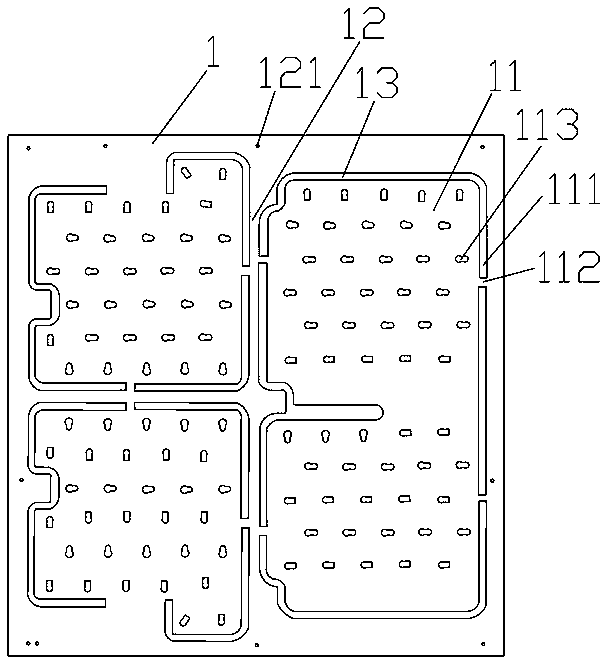
Figure 1 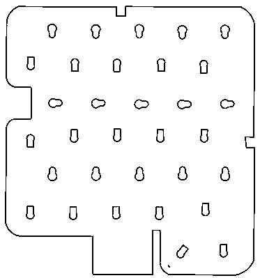
Figure 2 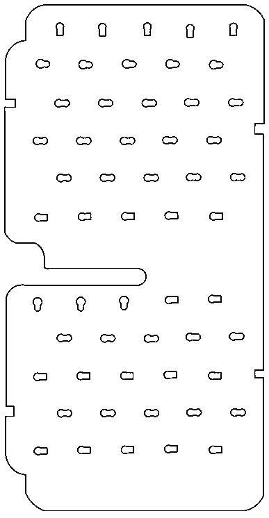
Figure 3
Abstract
Description
Technical field
[0001] The invention belongs to the technical field of circuit board production, and specifically relates to a method for manufacturing thick copper plates of different types of circuit boards and circuit boards. Background technique
[0002] With the continuous development of the circuit board industry, circuit boards for various purposes have also appeared. In recent years, due to the increasing international and domestic attention to environmental protection issues and the adjustment of national strategies, the rapid development of new energy electric vehicles and electric vehicle industries has been promoted as well as their applications in the new energy electric vehicles and electric vehicle industries. Circuit board technology for high-current and high-voltage battery protection has also grown rapidly.
[0003] Since the power battery protection circuit board needs to carry high current and high voltage, ordinary circuit boards can no longer meet this requir...
Examples
Embodiment Construction
[0023] In order to allow those skilled in the art to better understand the technical solutions of the present invention, the present invention will be further described with reference to the accompanying drawings.
[0024] Such as figure 1 As shown, a thick copper plate of a different type of circuit board includes a thick copper plate 1 with a square structure with a thickness of 1.0-1.2 mm. In order to improve the utilization of thick copper plates and save production materials, a plurality of thick copper plate units 11 corresponding to different types of circuit boards and a connection area 12 connecting each thick copper plate unit are provided on the thick copper plate 1 through the connection area 12 The connection makes each thick copper plate unit connected to the entire thick copper plate and has an integrated structure. The outer side of each thick copper plate unit 11 is provided with a gong edge 111 and a connecting position 112, and each thick copper plate is separa...