
A kind of LED chip with ITO film structure and preparation method thereof
A LED chip and thin film structure technology, applied in the direction of electrical components, circuits, semiconductor devices, etc., can solve the problems of metal electrode layer shedding, metal electrode layer pad performance AlGaInP-based chip reliability, ITO film layer shedding and other problems, Achieve the effects of reducing contact voltage, improving adhesion and integrity, and improving reliability of welding wires
Patent Information
- Authority / Receiving Office
- CN · China
- Patent Type
- Patents(China)
- Current Assignee / Owner
- Publication Date
- 2018-05-29
Smart Images
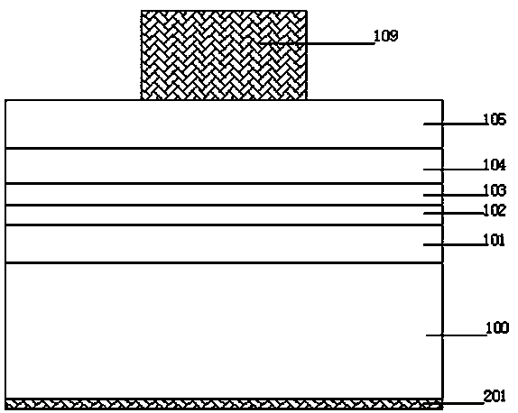
Figure 1 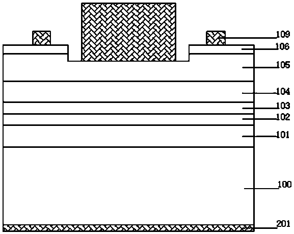
Figure 2 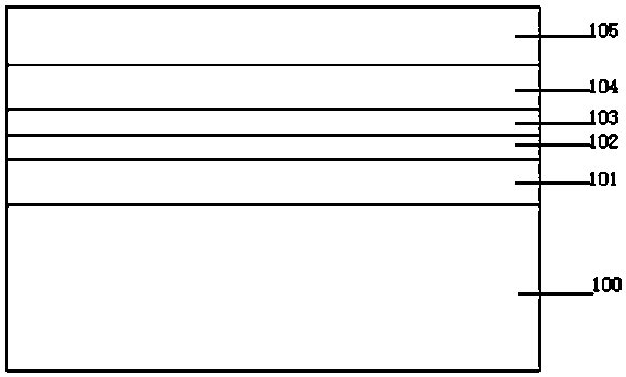
Figure 3
Abstract
Description
technical field
[0001] The invention relates to the field of semiconductor light emitting diodes, in particular to an LED chip with an ITO thin film structure and a preparation method thereof. Background technique
[0002] LED has the advantages of high light efficiency, low energy consumption, long life, high safety, and high environmental protection. It is a lighting method with broad application prospects, and has been valued by more and more countries. At present, LEDs have been widely used in the field of high-efficiency solid-state lighting, such as display screens, automotive lights, backlights, traffic lights, and landscape lighting.
[0003] Such as figure 1 As shown, a conventional AlGaInP light-emitting diode includes a GaAs substrate 100, a buffer layer 101, an n-AlGaInP confinement layer 102, an MQW multi-quantum well active layer 103, a p-AlGaInP confinement layer 104, and a p-GaP window layer 105, and a metal electrode layer 109 is directly disposed on the p...
Examples
Embodiment Construction
[0027] The present invention will be described in further detail below in conjunction with the embodiments and with reference to the accompanying drawings.
[0028] A kind of LED chip with ITO film structure, such as figure 2 As shown, a GaAs substrate 100 is included, and a buffer layer 101, an n-AlGaInP confinement layer 102, a multi-quantum well active layer 103, a p-AlGaInP confinement layer 104, and a p-GaP window layer are sequentially arranged on the GaAs substrate 100 105, an ITO film layer 106 is provided on the p-GaP window layer 105, a metal electrode layer 109 is provided on the ITO film layer 106, and a back electrode 201 is made under the GaAs substrate 100; the metal electrode layer 109 includes a main electrode and a For the extended electrodes, the main electrode is connected to the p-GaP window layer 105 , and the extended electrode is connected to the ITO thin film layer 106 .
[0029] A kind of preparation method of LED chip with ITO film structure, concr...