
Preparation method of N-type crystalline silicon cell, cell thereof, battery and system
A technology of crystalline silicon cells and crystalline silicon, applied in the field of solar cells, can solve the problems of incomplete removal, influence of PN junction quality, difficulty in guaranteeing phosphorus diffusion, etc., achieve high open circuit voltage and photoelectric conversion efficiency, good quality, and process Simple and Controllable Effects
Patent Information
- Authority / Receiving Office
- CN · China
- Patent Type
- Applications(China)
- Current Assignee / Owner
- Publication Date
- 2017-05-10
- Estimated Expiration
- Not applicable · inactive patent
Smart Images
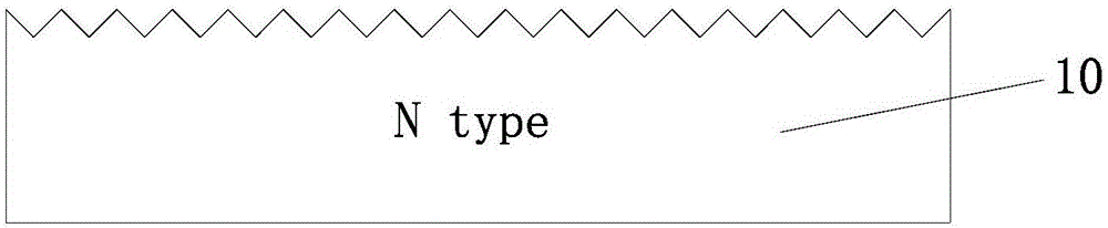
Figure 1 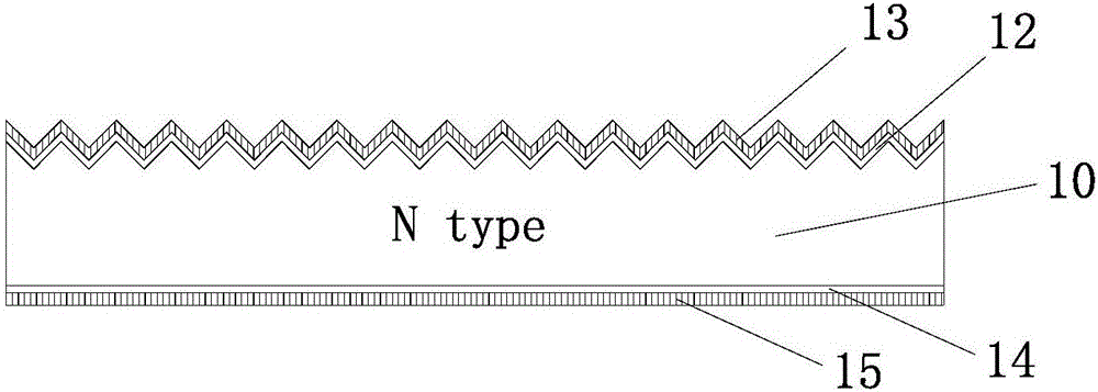
Figure 2 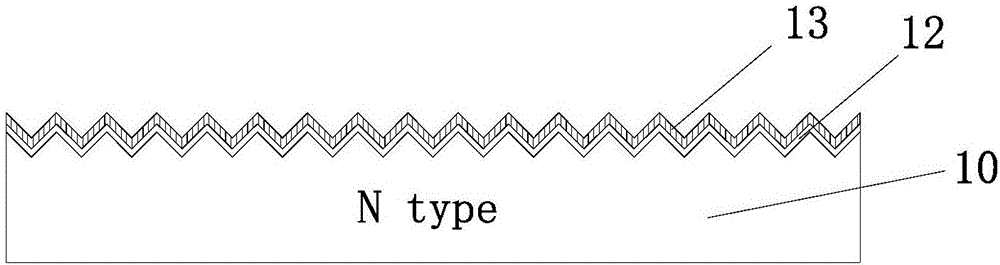
Figure 3
Abstract
Description
technical field
[0001] The invention relates to the technical field of solar cells, in particular to a method for preparing an N-type crystalline silicon cell and the cell, component and system thereof. Background technique
[0002] A solar cell is a semiconductor device that converts solar energy into electricity. At present, the mainstream products in the industry are P-type crystalline silicon solar cells. The battery process is simple, but it has a light-induced decay effect, that is, the efficiency of the battery will gradually decay with time, which is mainly due to the combination of boron atoms doped into the P-type silicon substrate and oxygen atoms in the substrate. Produces boron-oxygen pair results. Studies have shown that the boron-oxygen pair acts as a carrier trap, reducing the minority carrier lifetime, which leads to the attenuation of the photoelectric conversion efficiency of the battery. Compared with P-type crystalline silicon solar cells, N-type crys...
Examples
Embodiment Construction
[0044] The present invention will be described in detail below in conjunction with the embodiments and the accompanying drawings. It should be noted that the described embodiments are only intended to facilitate the understanding of the present invention, rather than limiting it in any way.
[0045] see Figure 1 to Figure 7 As shown, a method for preparing an N-type crystalline silicon battery provided in this embodiment includes the following steps:
[0046] (1), select the N-type crystalline silicon substrate 10 of 156.75mm * 156.75mm, and do texture processing to the front surface of the N-type crystalline silicon substrate 10; the resistivity of the N-type crystalline silicon substrate 10 is 0.2~15Ω·cm, Preferably 0.5-5Ω·cm; the thickness of the N-type crystalline silicon substrate 10 is 50-300 μm, preferably 80-200 μm; the battery structure after this step is as follows figure 1 shown.
[0047] (2) Put the N-type crystalline silicon substrate 10 treated in step (1) int...