
A Charge Pump with Wide Locking Range and Low Current Mismatch
A locking range and charge pump technology, applied in the field of microelectronics, can solve problems such as current mismatch, charge sharing, and restrictions on the application of charge pumps
Patent Information
- Authority / Receiving Office
- CN · China
- Patent Type
- Patents(China)
- Current Assignee / Owner
- Publication Date
- 2022-07-01
Smart Images
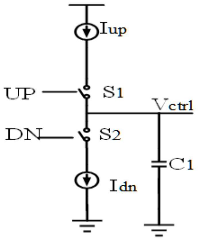
Figure 1 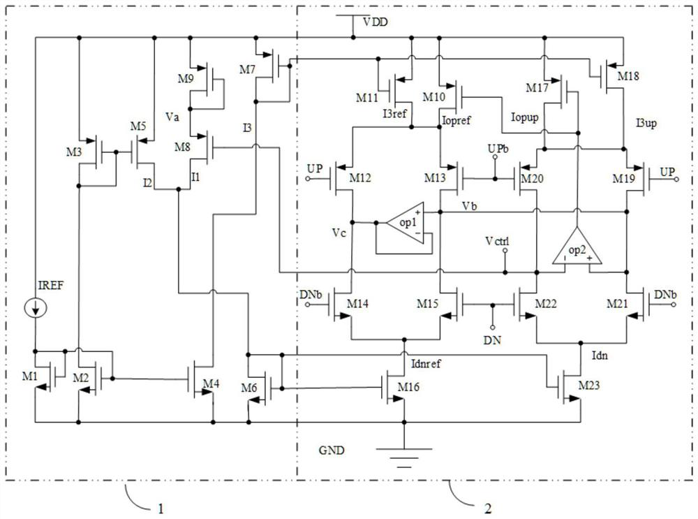
Figure 2 
Figure 3
Abstract
Description
technical field
[0001] The invention belongs to the technical field of microelectronics, and in particular relates to a charge pump with wide locking range and low current mismatch. Background technique
[0002] The charge pump is an important functional module of the delay-locked loop, and its performance directly affects the overall performance of the delay-locked loop. figure 1 It is a basic charge pump structure. When the switch S1 is closed and S2 is opened, the charging current source I UP When the capacitor C1 is charged, the voltage at the output terminal VCtrl of the charge pump rises; when the switch S1 is turned off and the switch S2 is turned on, the discharge current source I DN When the capacitor C1 is discharged, the voltage of the output terminal VCtrl of the charge pump drops; when the switch S1 and the switch S2 are turned on or off at the same time, the voltage of the output terminal VCtrl of the charge pump remains unchanged. figure 1 The conventional c...
Examples
Embodiment
[0021] A wide locking range low current mismatch charge pump such as figure 2 As shown, it includes a charge pump bias circuit 1 and a charge pump core circuit 2;
[0022] The signal output terminal of the charge pump bias circuit 1 is connected to the signal input terminal of the charge pump core circuit 2 , and the signal output terminal of the charge pump core circuit 2 is connected to the signal input terminal of the charge pump bias circuit 1 . terminal; the charge pump bias circuit 1 provides a bias signal for the charge pump core circuit 2, and the charge pump core circuit 2 provides charge / discharge current for the filter capacitor of the subsequent circuit.
[0023] As a preferred technical solution, such as figure 2 As shown, the charge pump bias circuit 1 includes: reference current source IREF, NMOS transistor M1, NMOS transistor M2, PMOS transistor M3, NMOS transistor M4, PMOS transistor M5, NMOS transistor M6, PMOS transistor M7, PMOS transistor M8 and PMOS t...