
RT detector suitable for epitaxial material and application thereof
A technology of epitaxial materials and detectors, which is applied in the direction of instruments, measuring devices, scientific instruments, etc., can solve the problems that the reflected signal exceeds the receiving range of the detector, the reflected signal exceeds the receiving range, and affects the accuracy, so as to realize the composition of the epitaxial layer and uniform growth control, avoid reflection signal out of control, and precisely control the effect of growth temperature
Patent Information
- Authority / Receiving Office
- CN · China
- Patent Type
- Applications(China)
- Current Assignee / Owner
- Publication Date
- 2021-08-13
- Estimated Expiration
- Not applicable · inactive patent
Smart Images
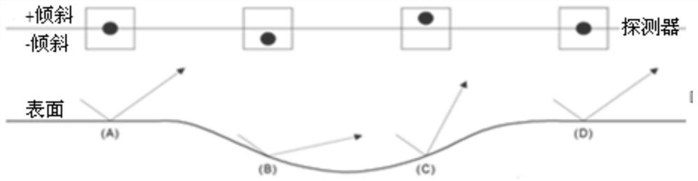
Figure 1 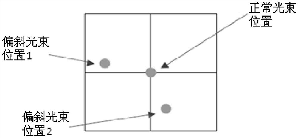
Figure 2 
Figure 3
Abstract
Description
technical field
[0001] The invention relates to the field of semiconductor material growth and preparation, in particular to an RT detector suitable for epitaxial materials and its application. Background technique
[0002] The growth and preparation of epitaxial materials by MOCVD requires precise monitoring of the growth temperature. There are two commonly used monitoring methods, namely (RT) and (TC). Among them, RT is the temperature of the wafer surface, which is realized by monitoring the reflectance curve, and TC is the temperature of the graphite disk, which is detected by a thermocouple.
[0003] Lattice-matched growth is a two-dimensional system produced by using heterostructures. It is mainly based on the fact that the atomic size of two different semiconductor materials is similar, so that semiconductor junctions close to perfect lattice matching can be produced, and the costs are not equal to each other. The meter energy levels will be aligned with each other ...
Examples
Embodiment 2
[0046] Embodiment 2 of the present invention is: a method for using an RT detector suitable for epitaxial materials, the method comprising the following steps:
[0047] placing the epitaxial wafer in the epitaxial wafer carrier, and controlling the motion state of the epitaxial wafer to be consistent with the carrier;
[0048] Adjust the monitoring mode in the RT detector according to the growth state of the epitaxial wafer to observe the growth process of the epitaxial wafer; wherein, the adjustment of the monitoring mode is to calculate the warping degree and Deformation feature, through the stepping motor to adjust the light direction of the eye-shaped light source.
Embodiment 3
[0049] Embodiment three of the present invention is: a method for using an RT detector suitable for epitaxial materials, the method comprising the following steps:
[0050] placing the epitaxial wafer in the epitaxial wafer carrier, and controlling the motion state of the epitaxial wafer to be consistent with the carrier;
[0051]Adjust the monitoring mode in the RT detector according to the growth state of the epitaxial wafer to observe the growth process of the epitaxial wafer; wherein, the adjustment of the monitoring mode is to calculate the degree of warpage and the intensity of the light received by the receiver. Deformation characteristics, change the position of light output by rotation, and record the direction of light output in polar coordinates.
[0052] The method for calculating the degree of warpage of the epitaxial wafers in Examples 2 and 3 of the present invention is as follows:
[0053] The position of the reflected light spot detected by the receiver is in...