
A kind of soi structure and manufacturing method, mems device and manufacturing method
A manufacturing method and device technology, applied in the field of SOI structure and manufacturing, and MEMS devices, can solve the problems of inability to effectively improve device reliability, poor insulation of isolation trenches, etc.
Patent Information
- Authority / Receiving Office
- CN · China
- Patent Type
- Patents(China)
- Current Assignee / Owner
- Publication Date
- 2021-11-16
Smart Images
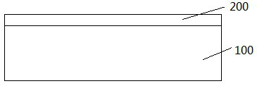
Figure 1 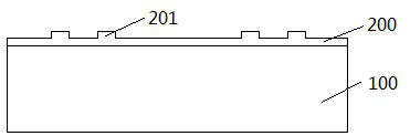
Figure 2 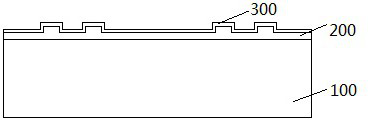
Figure 3
Abstract
Description
Technical field
[0001] The present invention relates to a semiconductor manufacturing technology, and more particularly relates to a method for producing an SOI structure and, further relates to a MEMS device formed by the SOI structure and a manufacturing method of the MEMS device. Background technique
[0002] SOI (Silicon-On-Insulator) on the insulating layer of silicon that is, the technology is between the top layer and the back silicon substrate having a silicon layer of a multilayer structure introduces a buried oxide layer is formed. Due to the unique advantages of SOI structures, devices based on this structure will be essentially reduced junction capacitance and leakage current, increase switching speed, lower power consumption, high speed, low power operation, which is superior to bulk silicon devices and circuit. SOI structure currently used for manufacturing most of the devices have been widely used in the field of microelectronics, optoelectronics while still other ...
Examples
Embodiment Construction
[0044] The technical solutions in the embodiments of the present invention will be apparent from the drawings in the embodiment of the present invention.
[0045] The following examples are deployed as an example of an SOI structure to achieve an isolation insulation application, first disclosed a SOI structure and a method of manufacturing the SOI structure, wherein the SOI structure is Image 6 As shown, the uppermost and upper, at least the first silicon layer 100, the insulating layer, and the second silicon layer 500 are included. The SOI structure (on the insulator) is often used in the manufacture of the MEMS device, mainly using the intermediate blankets to achieve insulation isolation between the electrodes. Unlike the existing SOI structure, a silica monolayer structure is used to form a blade layer. The insulating layer in the present embodiment is combined with a plurality of different material insulating materials, and the multilayers here are at least three layers, ie...