
Wide bandgap semiconductor double-sided heat dissipation module packaging structure based on conductive metal band
A wide-bandgap semiconductor and conductive metal strip technology, applied in semiconductor devices, semiconductor/solid-state device components, and electrical solid-state devices, etc., can solve the problems of bond point connection failure, harsh heat dissipation environment, and large chip thermal resistance. Enhance current flow capacity, improve space utilization, reduce the effect of common source inductance
Patent Information
- Authority / Receiving Office
- CN · China
- Patent Type
- Applications(China)
- Current Assignee / Owner
- Publication Date
- 2022-06-21
Smart Images
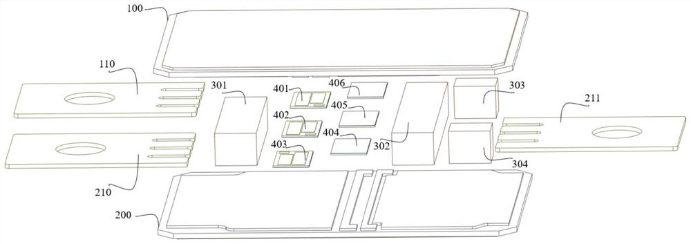
Figure 1 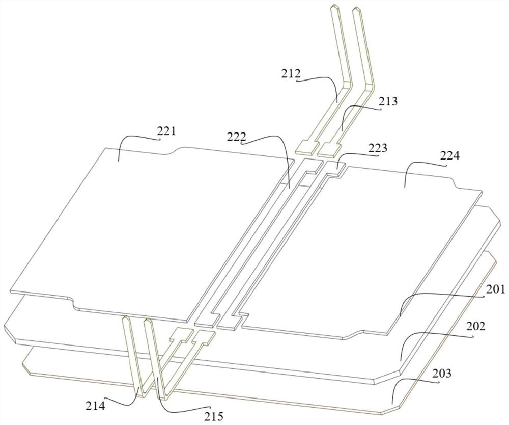
Figure 2 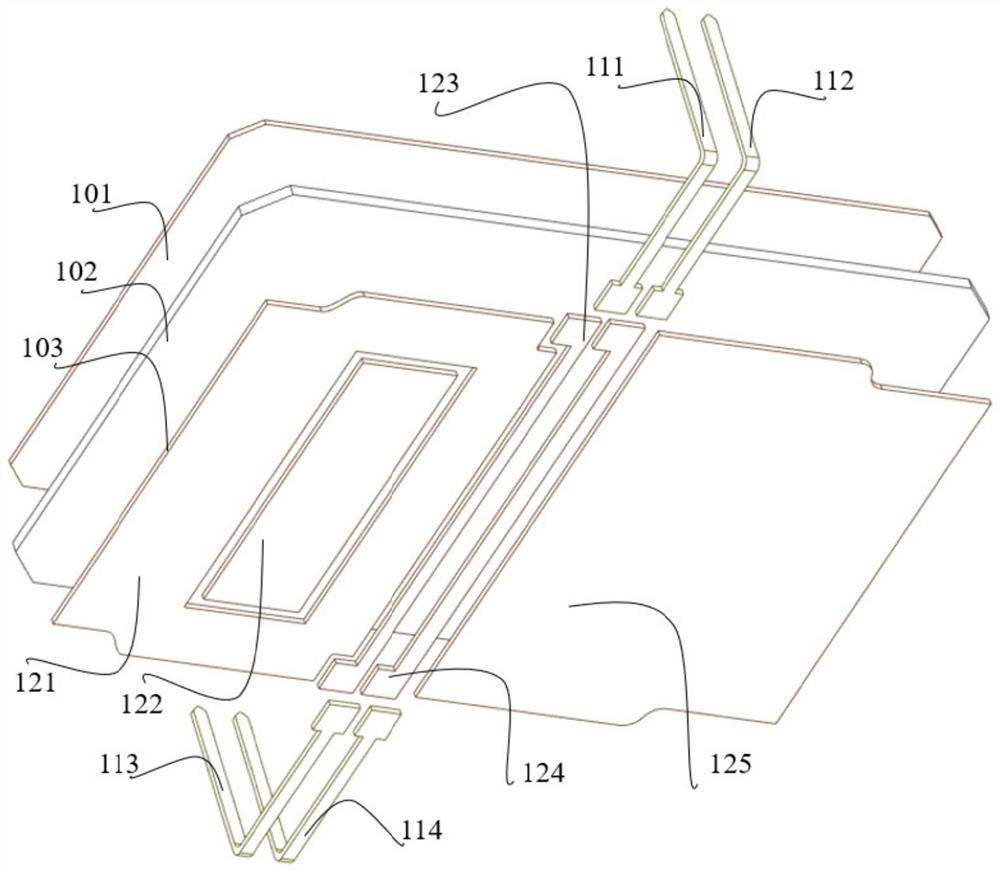
Figure 3
Abstract
Description
technical field
[0001] The invention belongs to the technical field of semiconductor packaging, and in particular relates to a wide-bandgap semiconductor double-sided heat dissipation module packaging structure based on conductive metal strips. Background technique
[0002] A power module is a module formed by repackaging several power semiconductor chips according to a certain functional combination. Compared with discrete power devices, power modules have a high degree of integration, so they have great advantages in electrical performance, thermal performance and economic considerations.
[0003] In recent years, with the rapid development of industries represented by new energy grid connection, high-voltage direct current transmission, electric vehicles, high-speed rail, aerospace, and pulse power, the performance requirements of power electronic systems for semiconductor power modules are increasing, which promotes the continuous improvement of power modules. It is dev...
Examples
Embodiment
[0067] see figure 1 , figure 2 , image 3 and Figure 4 , the package structure of this embodiment includes 2 power substrates, 2 groups of 6 wide bandgap power semiconductor chips, 4 power pads, 3 power terminals, 8 drive terminals and 6 groups of conductive metal strips.
[0068] The two power substrates are specifically the top power substrate 100 and the bottom power substrate 200 .
[0069] The six wide-bandgap power semiconductor chips 400 are specifically a first high-arm wide-bandgap power semiconductor chip 401, a second high-arm wide-bandgap power semiconductor chip 402, a third high-arm wide-bandgap power semiconductor chip 403, The first lower arm wide bandgap power semiconductor chip 404 , the second lower arm wide bandgap power semiconductor chip 405 and the third lower arm wide bandgap power semiconductor chip 406 .
[0070] The four power pads are specifically a DC side power pad 301 , an AC side main power pad 302 , an AC side auxiliary power pad 303 and ...