
Solid-state imaging device and method for manufacturing the same
A solid-state imaging device, a horizontal technology, applied in the direction of electric solid-state devices, radiation control devices, semiconductor devices, etc., can solve the problems of limited drive pulse delay, inability to increase, and dielectric breakdown strength (reduced insulation withstand voltage, etc.)
Patent Information
- Authority / Receiving Office
- CN · China
- Patent Type
- Applications(China)
- Current Assignee / Owner
- Publication Date
- 2007-04-25
- Estimated Expiration
- Not applicable · inactive patent
Smart Images
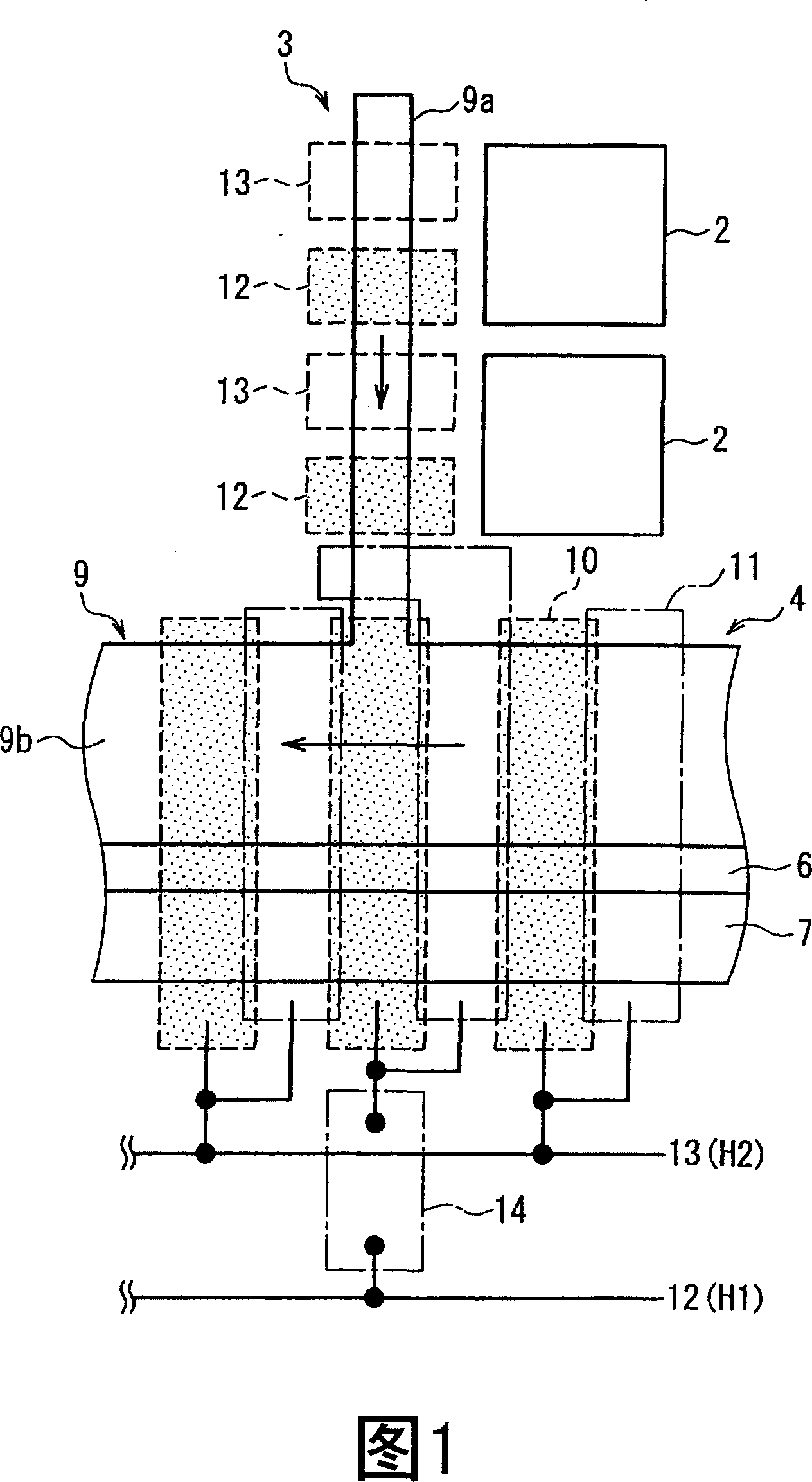
Figure 1 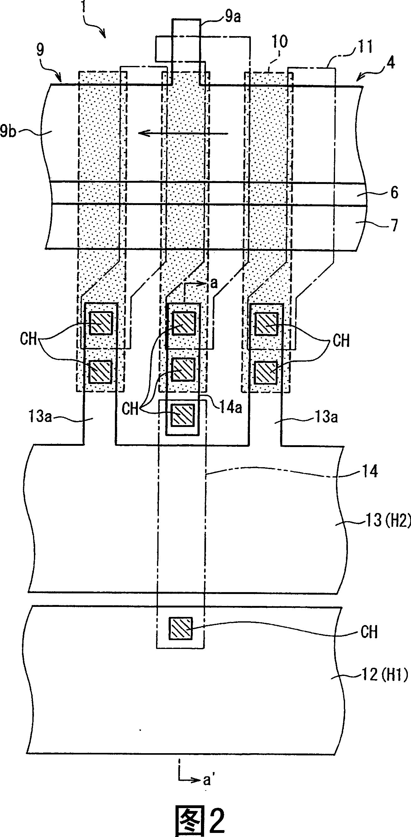
Figure 2 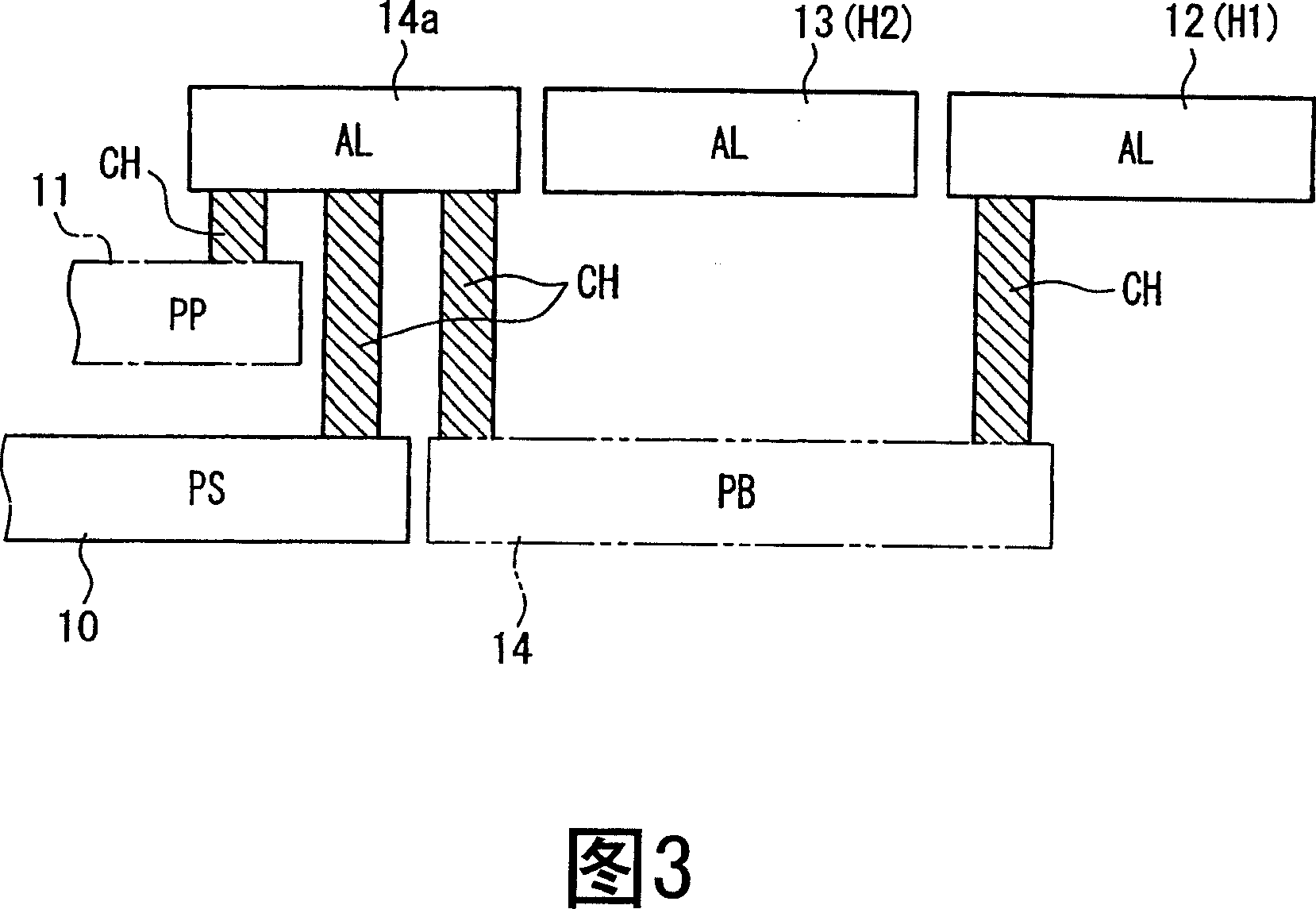
Figure 3
Abstract
Description
technical field
[0001] The present invention relates to a solid-state imaging device and a manufacturing method thereof, and more particularly to a CCD (CHARGE COUPLING DEVICE: Charge Coupled Device) type solid-state imaging device and a manufacturing method thereof. Background technique
[0002] In recent years, solid-state imaging devices are mounted on digital cameras and digital video cameras, and demand is increasing. In addition, among portable terminal devices typified by mobile phones, there are more and more types having a camera function. Demand for solid-state imaging devices has also increased as imaging devices for such portable terminal devices. Furthermore, in order to obtain high-quality images, the number of pixels of solid-state imaging devices tends to increase. In addition, with the reduction in power consumption of digital cameras, digital video cameras, portable terminal devices, and the like, there is an increasing demand for low power consumption of...
Examples
Embodiment approach 1
[0044] FIG. 1 is a plan view schematically showing the configuration of a solid-state imaging device according to Embodiment 1 of the present invention.
[0045] As shown in FIG. 1 , the solid-state imaging device according to Embodiment 1 is a CCD-type solid-state imaging device formed on a semiconductor substrate. Similar to the conventional examples shown in FIGS. 6 to 8 in the description of the background art, a plurality of light receiving sections 2 arranged in a two-dimensional matrix and a plurality of light receiving sections 2 along the semiconductor substrate (101 in FIG. 6 ) are provided on a semiconductor substrate (101 in FIG. 6 ). The vertical transfer unit (vertical CCD) 3 is arranged for each column in the vertical direction. In addition, a horizontal transfer unit (horizontal CCD) 4 is provided so as to be adjacent to the final row of the vertical transfer unit 3 .
[0046] The light receiving unit 2 is constituted by a photodiode, and stores charges accord...
Embodiment approach 2
[0057] 5 is a plan view schematically showing the configuration of a solid-state imaging device according to a second embodiment of the present invention.
[0058] As shown in FIG. 5 , in the solid-state imaging device of the present embodiment, a discharge region connection portion 15 for applying a voltage to the discharge region 7 is provided for each horizontal CCD 4 , and a connection between the discharge region connection portion 15 and the power supply line is provided. The discharge contact area 16 of the connecting portion.
[0059] By disposing in this way, with respect to the discharge region 7, it is possible to suppress an increase in impurities due to deterioration of the withstand voltage due to a decrease in the resistance value that determines the discharge capability, or an increase in the discharge area due to an increase in the load capacitance. . As a result, the area of the thin film region of the insulating film covering the horizontal transfer elect...