
Semiconductor device having shallow trenches and method for manufacturing the same
a semiconductor device and shallow trench technology, applied in the field of semiconductor devices, can solve the problems of worsening the switching characteristics of semiconductor devices
Patent Information
- Authority / Receiving Office
- US · United States
- Patent Type
- Applications(United States)
- Current Assignee / Owner
- Publication Date
- 2005-01-27
- Estimated Expiration
- Not applicable · inactive patent
Smart Images
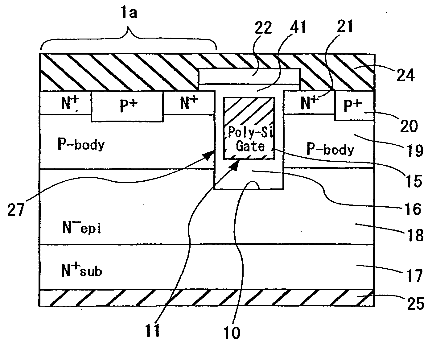
Figure 1 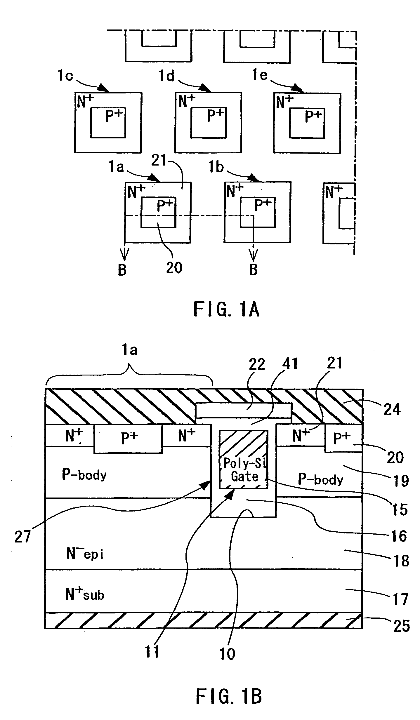
Figure 2 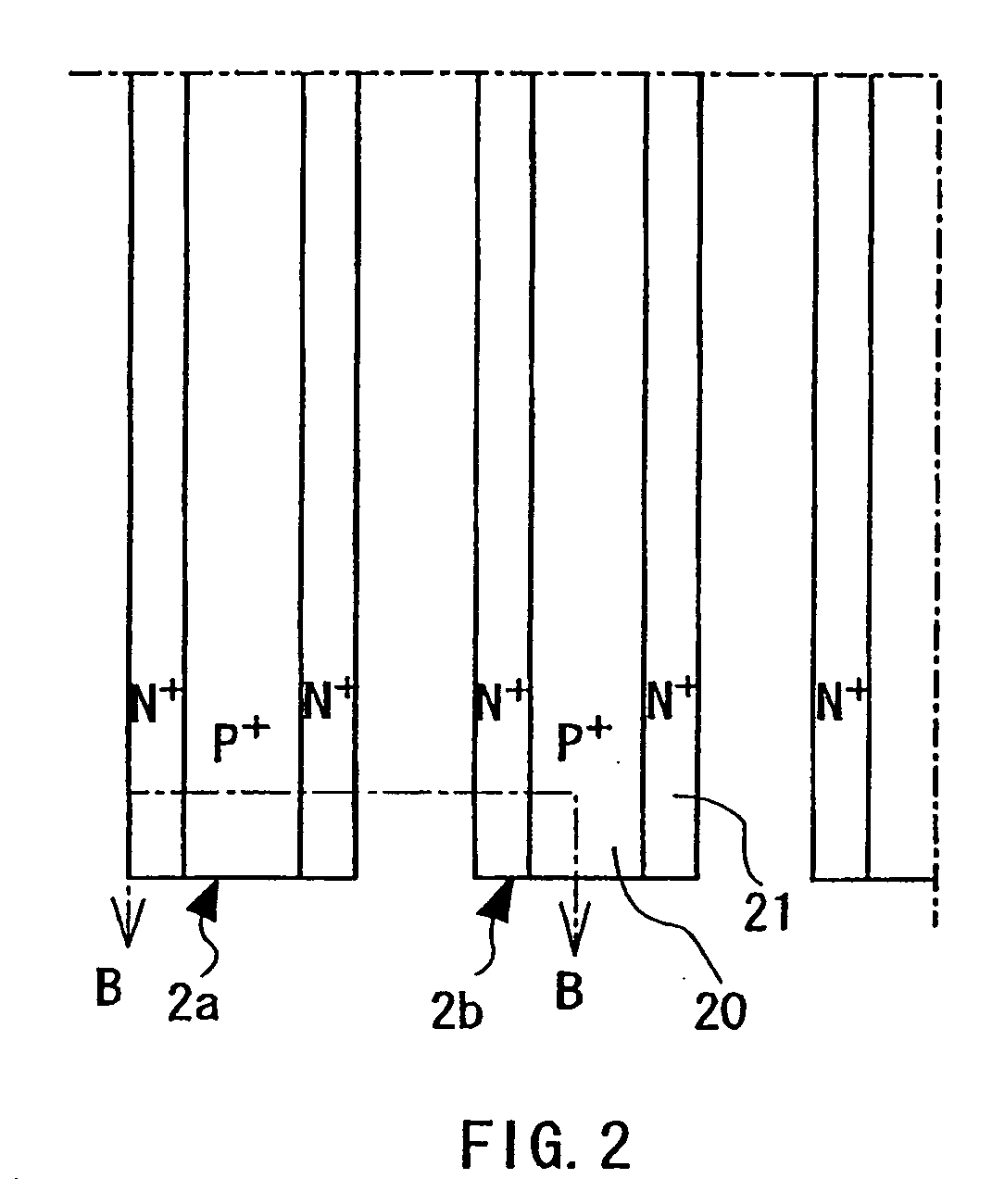
Figure 3
Abstract
Description
BACKGROUND OF THE INVENTION
[0001] 1. Field of the Invention
[0002] The present invention relates to a semiconductor device and a method of manufacturing the same. In particular, the present invention relates to a semiconductor device with a trench gate power MOSFET construction that is used in a power supply circuit or the like, and to a method of manufacturing the same.
[0003] 2. Background Art
[0004] Trench gate power MOSFETs have been widely used in recent years in a variety of power supply apparatuses, such as DC-DC converters. FIGS. 51A and 51B show one example of a semiconductor device that has a trench gate power MOSFET construction according to the background art, with FIG. 51A being an overhead view of the semiconductor device and FIG. 51B being a cross-sectional view taken along the line A-A in FIG. 51A. In these drawings, numerals 100a to 100e are cells, numeral 110 is a trench, numeral 111 is a gate electrode film, numeral 117 is an N+ type silicon substrate, numeral 11...
Examples
first embodiment
[0074] The following is a detailed description, with reference to the attached drawings, of a semiconductor device that is a first embodiment of the present invention. FIGS. 1A and 1B show a semiconductor device of this first embodiment of the present invention, with FIG. 1A being an overhead view showing the arrangement of the cells of the semiconductor device and FIG. 1B being a cross-sectional view taken along the line B-Bin FIG. 1A. In these drawings, numerals 1a to 1e are cells, numeral 10 is a trench, numeral 11 is a gate electrode film, numeral 15 is a side surface part, numeral 16 is a bottom surface part, numeral 17 is an N+ type silicon substrate, numeral 18 is an N− epitaxial layer, numeral 19 is a P type body layer, numeral 20 is a P+type diffusion region, numeral 21 is an N+type source region, numeral 22 is an interlayer dielectric, numeral 24 is a source electrode film, numeral 25 is a drain electrode film, numeral 27 is a gate insulating film, and numeral 41 is an upp...
second embodiment
[0098] The following is a detailed description, with reference to the attached drawings, of a semiconductor device that is a second embodiment of the present invention. FIG. 22 is a cross-sectional view of a semiconductor device of this second embodiment of the present invention. In this drawing, numerals 1a to 1e are cells, numeral 12 indicates gate electrode film upper parts, numeral 13 indicates gate electrode film lower parts, numeral 14 indicates lower side surface parts, and numeral 29 indicates upper side surface parts. The other numerals denote the same parts as in FIG. 1.
[0099] As shown in FIG. 22, the cross-sectional form of the semiconductor device of this second embodiment of the present invention is such that the lower side surface parts 14 of the gate insulating film 27 are thicker than the upper side surface parts 29 of the gate insulating film 27. As a result, the gate electrode film upper parts 12 are thicker than the gate electrode film lower parts 13. The remaini...
third embodiment
[0119] The gate electrode film 11 was described as being formed with stepped sides so that there are two parts with different thicknesses, though the gate electrode film 11 may be formed with a higher number of parts with different thicknesses. FIG. 49 is a cross-sectional drawing showing a semiconductor device according to a third embodiment of the present invention. The numerals used in FIG. 49 are the same as those used in FIG. 1. As shown in FIG. 49, the semiconductor device according to the third embodiment of the present invention has a gate electrode film 11 that has three vertically arranged parts with different thicknesses.