
[multi-chip package and manufacturing method thereof]
a manufacturing method and multi-chip technology, applied in the direction of semiconductor devices, semiconductor/solid-state device details, electrical apparatus, etc., can solve the problems of time-consuming and highly inefficient manufacturing process, and the distortion of internal signal transmission of multi-chip packages, so as to shorten the inter-chip connection pathway and improve the signal transmission quality of the package
Patent Information
- Authority / Receiving Office
- US · United States
- Patent Type
- Applications(United States)
- Current Assignee / Owner
- Publication Date
- 2005-02-10
Smart Images
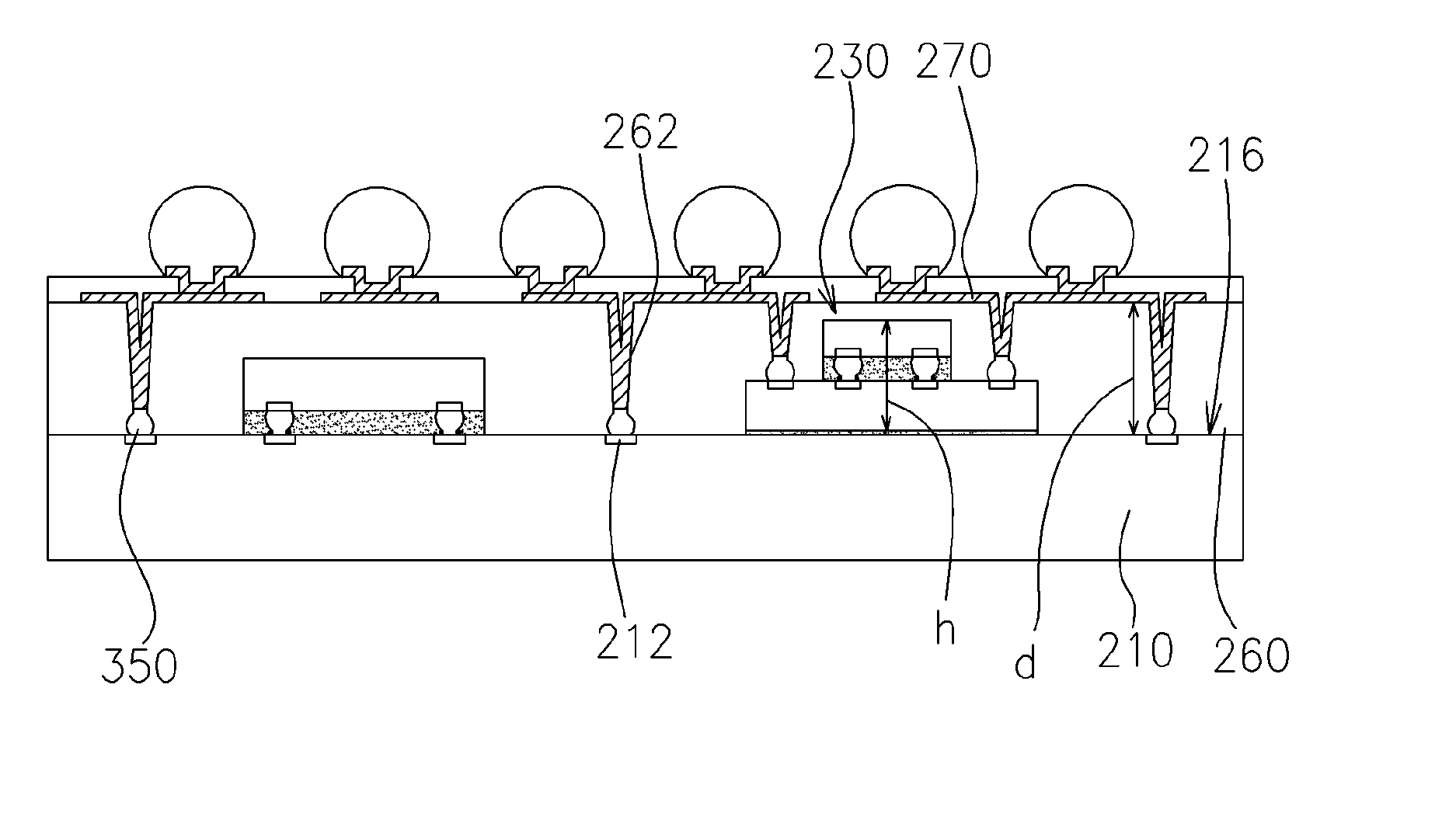
Figure 1 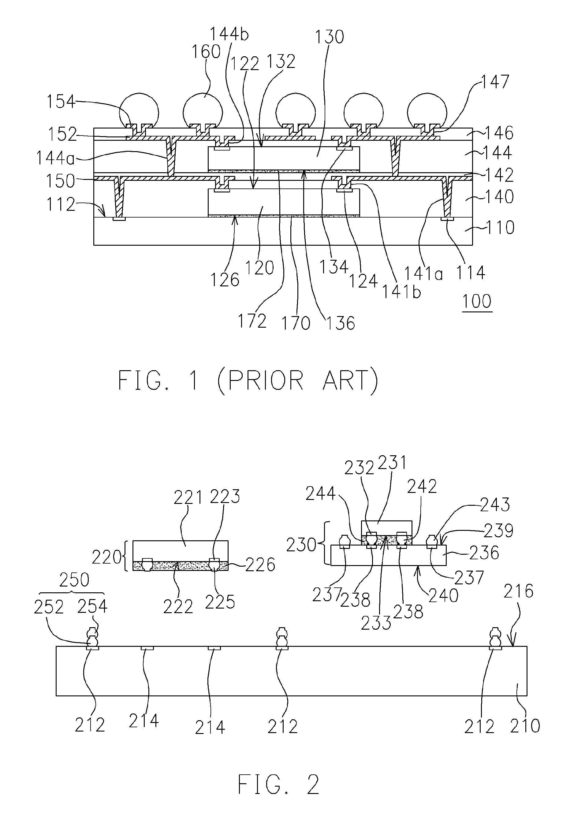
Figure 2 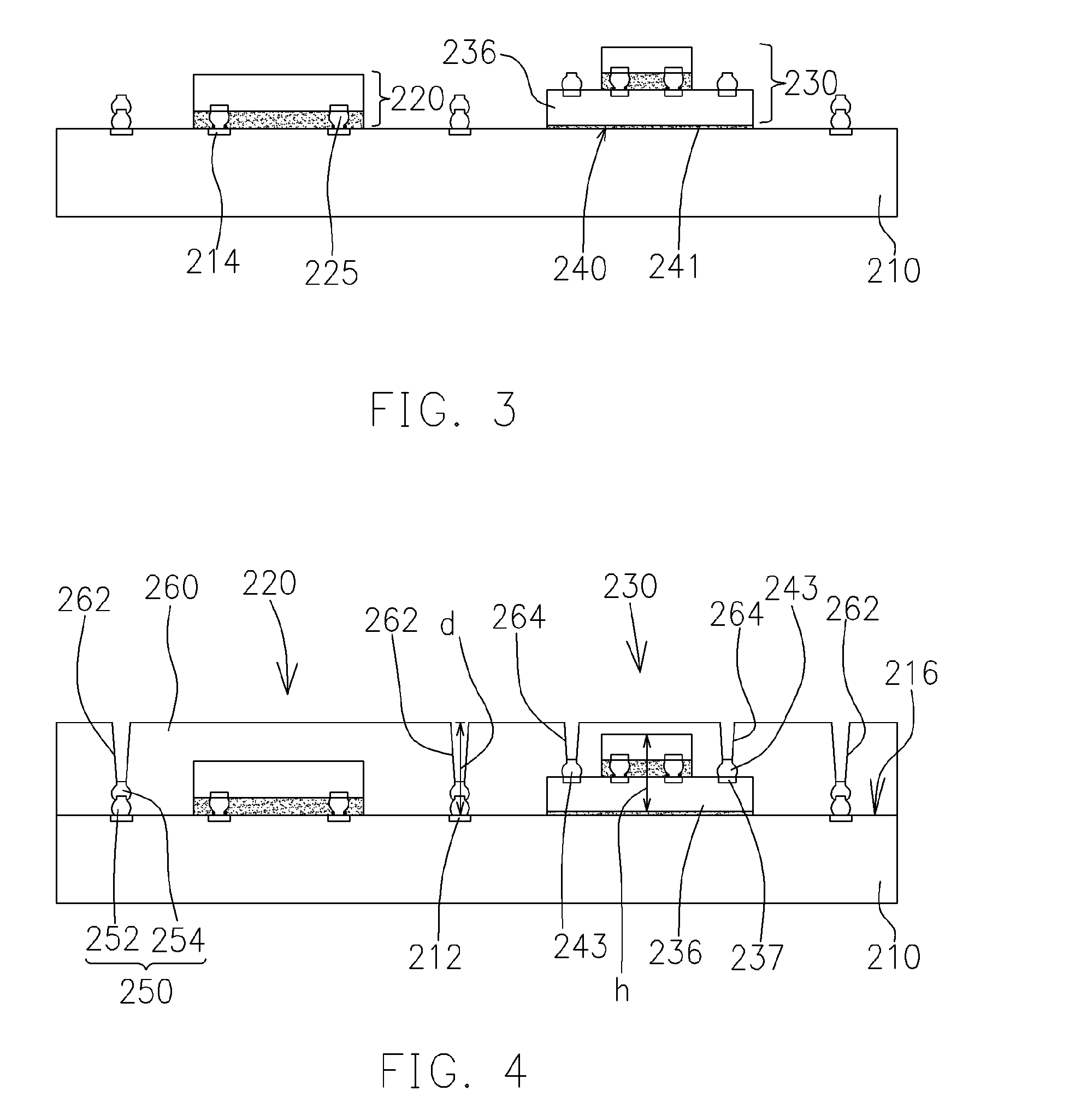
Figure 3
Abstract
Description
CROSS REFERENCE TO RELATED APPLICATIONS
[0001] This application claims the priority benefit of Taiwan application serial no. 92121788, filed Aug. 8, 2003. BACKGROUND OF INVENTION
[0002] 1. Field of the Invention
[0003] The present invention relates to a multi-chip package and manufacturing method thereof. More particularly, the present invention relates to a high electrical performance multi-chip package that can be manufactured with fewer processing steps.
[0004] 2. Description of the Related Art
[0005] In this information-centered society, everyone is shopping around for high speed, high quality, and multifunctional products. As far as aesthetic appearance is concerned, most products are designed to be slim, compact, light and easy to use. In order to achieve the above goals, most manufacturers will incorporate system design concepts into their products so that a single chip can have a variety of functions. Ultimately, the total number of chips inside each electrical product and t...
Examples
Embodiment Construction
[0023] Reference will now be made in detail to the present preferred embodiments of the invention, examples of which are illustrated in the accompanying drawings. Wherever possible, the same reference numbers are used in the drawings and the description to refer to the same or like parts.
[0024] FIGS. 2 to 8 are schematic cross-sectional views showing the progression of steps of fabricating a multi-chip package according to a first preferred embodiment of this invention. As shown in FIG. 2, a carrier 210, a first package module 220 and second package module 230 are provided. The carrier 210 can be a chip (an active device) or an integrated circuit (IC) package substrate (for example, a glass substrate, a ceramic substrate or a polymer substrate), wherein passive devices can be embedded in the substrate. The carrier 210 has a plurality of bonding pads 212, 214 located on a surface 216. A plurality of contacts 250 is formed on the surface of the respective bonding pads 212. Each conta...