

Abrasive particles, polishing slurry, and producing method thereof
a technology of polishing slurry and abrasive particles, which is applied in the field of slurry, can solve the problems of reducing the removal speed of the oxide layer, the removal speed of the nitride layer, and the scratching surface of the wafer, and achieve the effect of minimizing micro scratches
Patent Information
- Authority / Receiving Office
- US · United States
- Current Assignee / Owner
- Publication Date
- 2006-07-20
- Estimated Expiration
- Not applicable · inactive patent
Smart Images
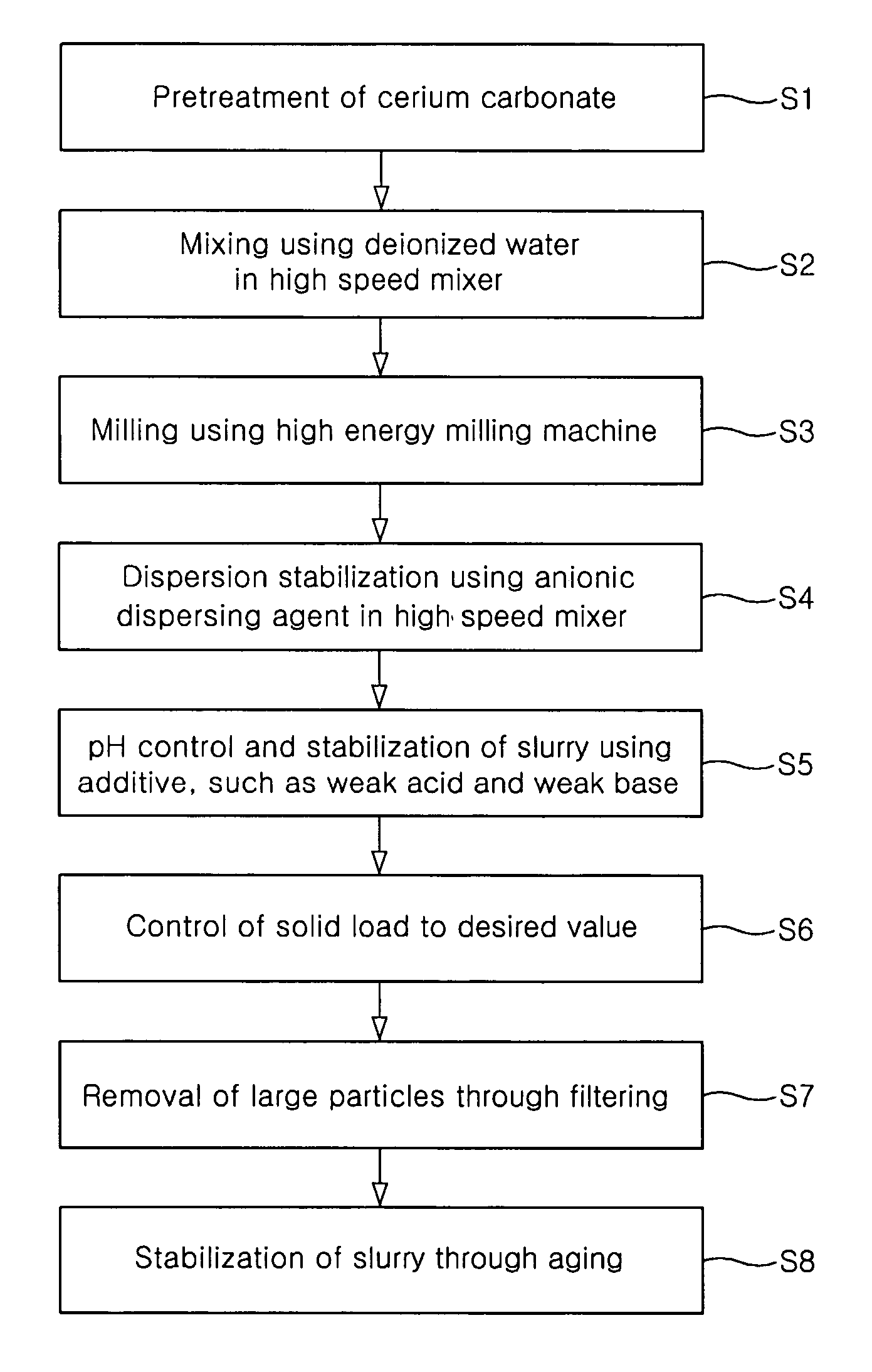
Figure 1 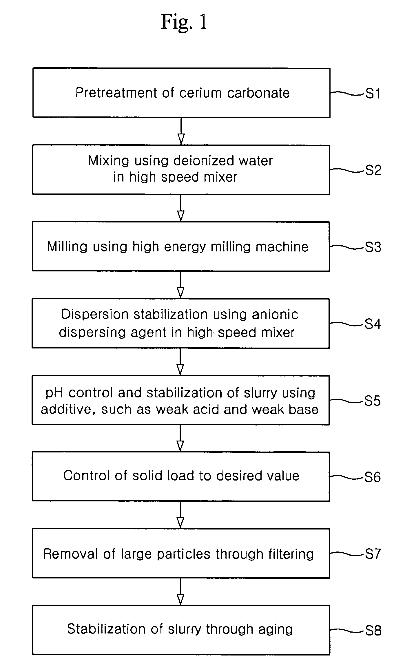
Figure 2 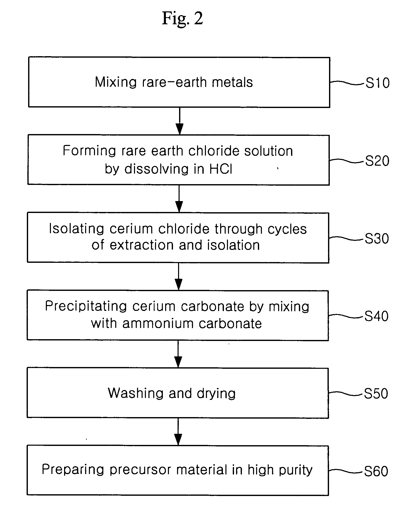
Figure 3
Abstract
Description
[0001] This application claims the priority of Korean Patent Application No. 10-2004-0107276, filed on Dec. 16, 2004 and 10-2005-0063665, filed on Jul. 14, 2005 in the Korean Intellectual Property Office, the disclosures of which are incorporated herein in their entirety by reference. BACKGROUND OF THE INVENTION
[0002] 1. Field of the Invention
[0003] The present invention relates to a slurry for use in a chemical mechanical polishing (hereinafter, referred to as ‘CMP’) process. More particularly, the present invention relates to a polishing slurry for use in a shallow trench isolation (STI) CMP process, necessary for fabricating ultra highly integrated semiconductors of 256 mega D-RAM or more (Design rule of 0.13 μm or less), which can polish wafers at a high removal rate, having an excellent the removal selectivity of oxide compared to nitride, abrasive particles therefore, and methods for producing the abrasive particles and the polishing slurry.
[0004] 2. Description of the Rela...
Examples
Embodiment Construction
[0044] Hereinafter, a process of producing a polishing slurry according to the present invention will be described in detail separately from the analysis of properties of the polishing slurry. Particularly, changes in the properties of the polishing slurry will be analyzed when agglomerates of the raw materials vary in size and when a multi-step calcination process is introduced, in separation. Furthermore, a description will be given of a method of producing the polishing slurry using ceria as a polishing agent, deionized water as a dispersion medium thereof, and an anionic polymer dispersing agent as a dispersing agent. Also, the CMP results, such as oxide film polishing speed and selectivity, depending on process conditions, will be given. Many modifications and variations of the present invention, which will be described later, are possible, and the scope of the present invention is not limited by the following description. [Production of Ceria Slurry]
[0045] The ceria slurry of ...