
Substrate based IC-package
Patent Information
- Authority / Receiving Office
- US · United States
- Current Assignee / Owner
- Publication Date
- 2007-02-01
- Estimated Expiration
- Not applicable · inactive patent
Smart Images
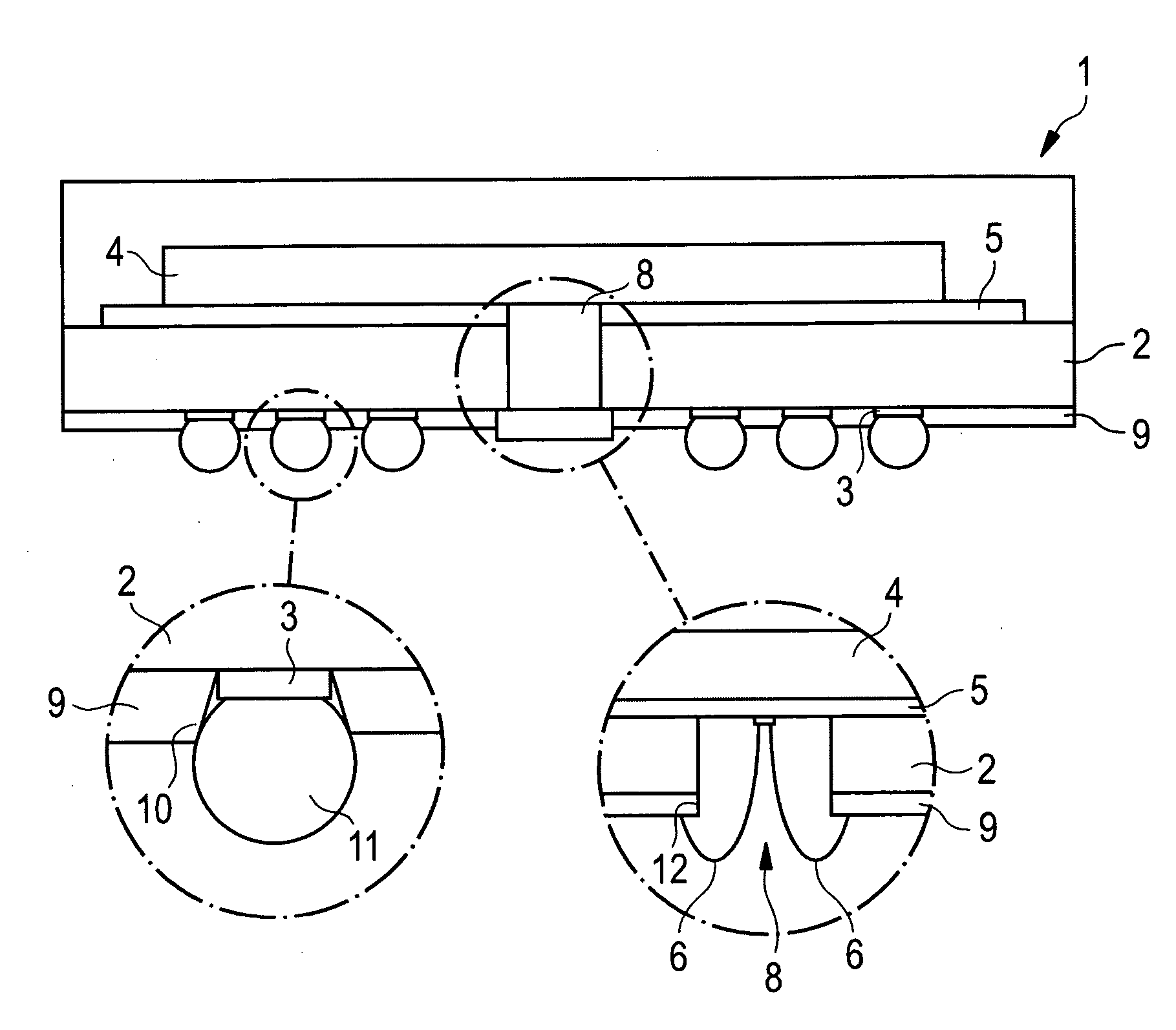
Figure 1 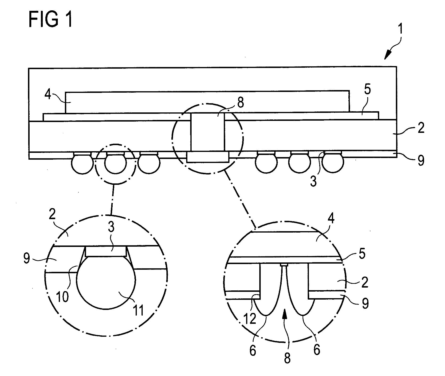
Figure 2 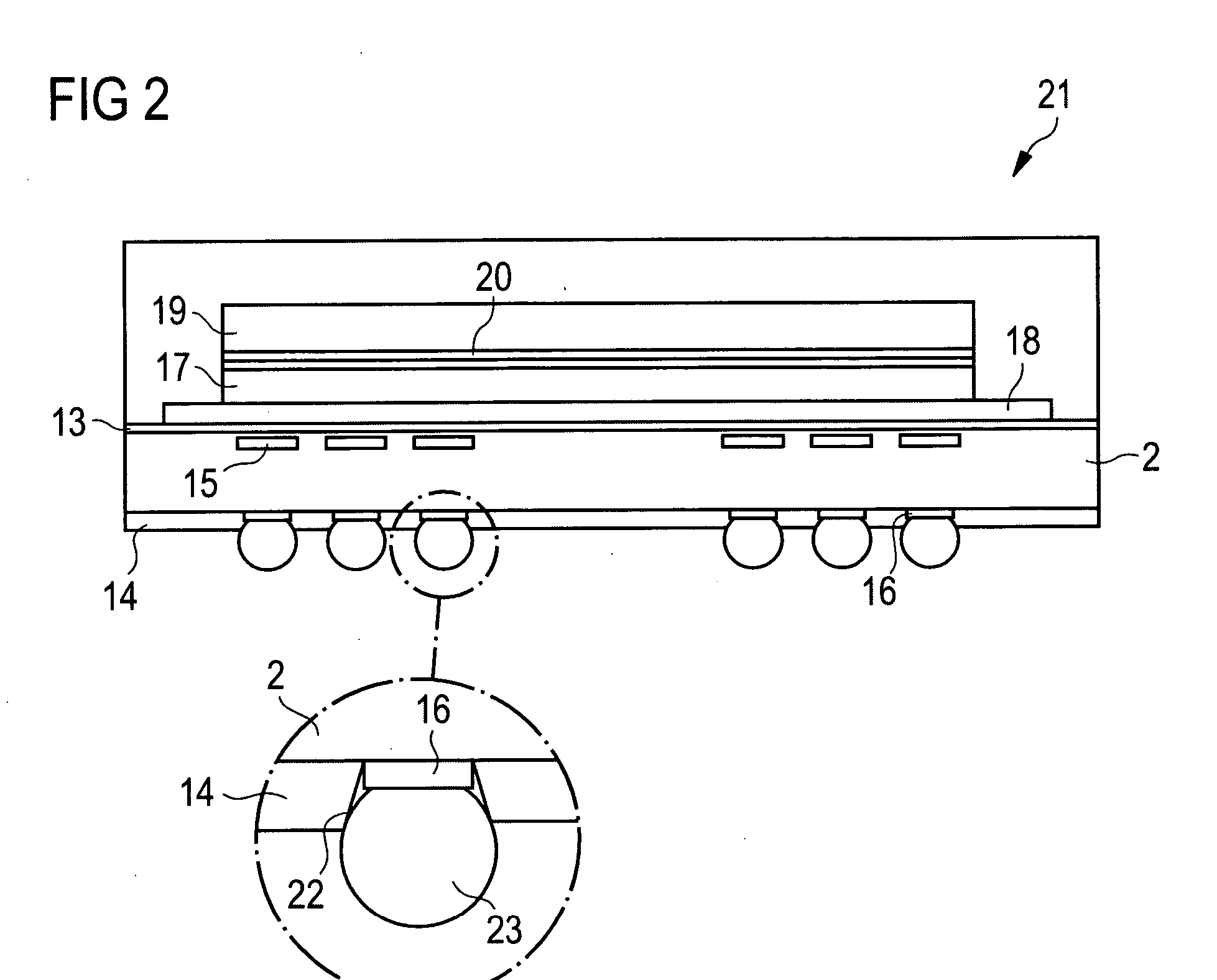
Figure 3
Abstract
Description
TECHNICAL FIELD
[0001] Generally to packaged integrated circuits and in more particular to a substrate based integrated circuit package. BACKGROUND
[0002] An IC-package, such as a ball grid array package, includes a substrate having a first surface and a second surface. A chip is mounted on a surface and ball pads, conducting traces and solder masks on the other surface wherein the conducting traces are disposed in between the adjacent ball pads, and are covered by the solder mask. A portion of each of the ball pads is also covered by the solder mask. The solder mask is produced by photolithographic structuring and developing of an epoxy resin.
[0003] The solder mask includes openings positioned in the area corresponding to the ball pads, wherein the opening exposes an opening of the surface of the substrate, the ball pad and a portion of the side wall of the wall pad. The chip is disposed on the second surface of the substrate and is sealed and encapsulated by the insulated materia...
Examples
Embodiment Construction
[0025] The making and using of the presently preferred embodiments are discussed in detail below. It should be appreciated, however, that the present invention provides many applicable inventive concepts that can be embodied in a wide variety of specific contexts. The specific embodiments discussed are merely illustrative of specific ways to make and use the invention, and do not limit the scope of the invention.
[0026] According to FIG. 1, the BOC (Board On Chip) package 1 includes a substrate 2 with contact pads 3 on one of its sides. The contact pads 3 are part of a not shown wiring on the substrate 2. The wiring is normally made of copper by a previous process. On the side opposite to the contact pads 3, a chip 4 is mounted with a die attach 5 between the substrate surface and the lower surface (active side of the chip) of the chip 4.
[0027] The chip 4 of this embodiment is provided with a central row of contact pads (not shown) which are connected via wire loops 6 with pads 7 o...