
Memory device etch methods
a memory device and etching technology, applied in the field of memory device etching, can solve the problems of reducing the geometry of the design feature below the critical dimension (cd), challenging the limitations of conventional methods, and the conventional photoresist material becomes too thin to sustain the resistance to the etch plasma during the etching process
Patent Information
- Authority / Receiving Office
- US · United States
- Patent Type
- Applications(United States)
- Current Assignee / Owner
- Publication Date
- 2008-06-26
Smart Images
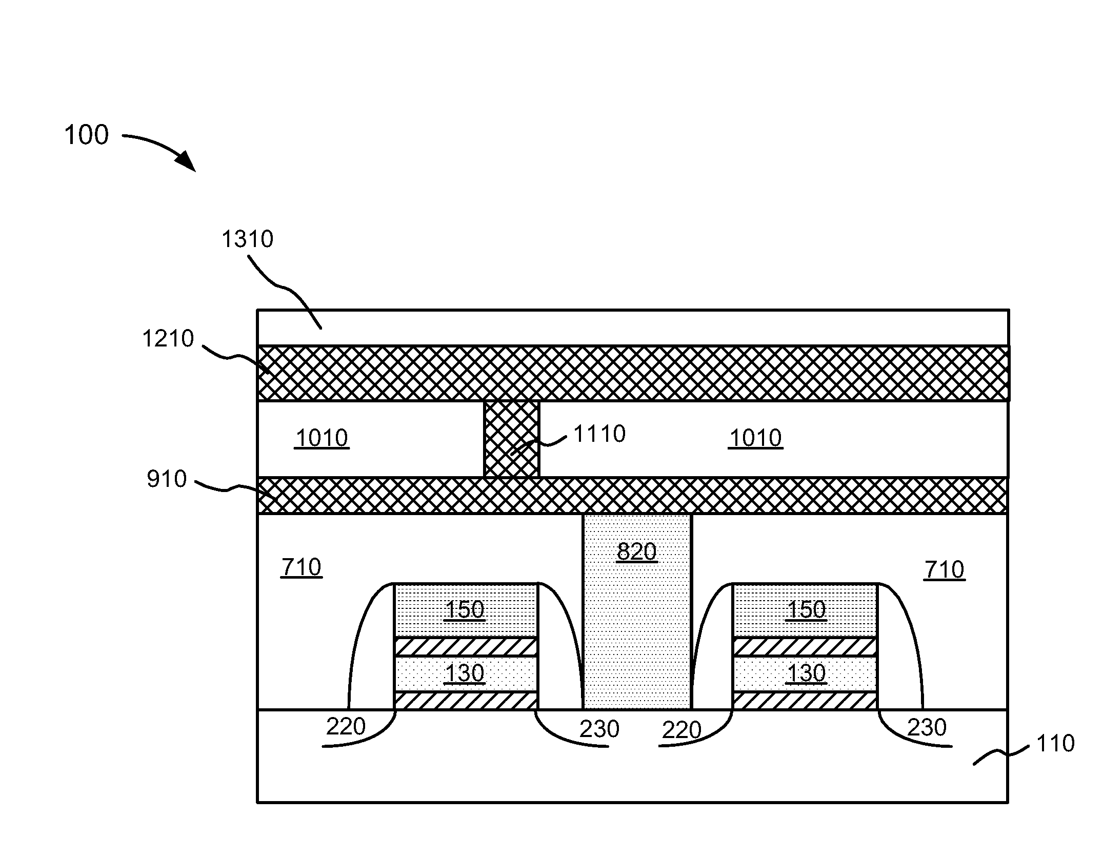
Figure 1 
Figure 2 
Figure 3
Abstract
Description
BACKGROUND
[0001] 1. Field of the Invention
[0002] Implementations described herein relate generally to methods of manufacturing semiconductor devices, and, more particularly, to etch methods for memory devices.
[0003] 2. Description of Related Art
[0004] The escalating demands for high density and performance associated with non-volatile memory devices require small design features, high reliability, and increased manufacturing throughput. The reduction of design features below a critical dimension (CD) challenges the limitations of conventional methodologies. The critical dimension of a semiconductor device design feature may be the length or width of that feature.
[0005] For example, etch methods may be used to form design features on memory devices. Typically, photoresist layers are patterned to define the design feature on the material to be etched. The photoresist layer may act as a mask to protect the portion of the material underlying the photoresist while leaving exposed the portion ...
Examples
Embodiment Construction
[0025]The following detailed description of the invention refers to the accompanying drawings. The same reference numbers in different drawings may identify the same or similar elements. Also, the following detailed description does not limit the invention.
[0026]Implementations consistent with principles of the invention may relate to hard mask etch methods that provide critical dimensions for memory cells used in memory devices. By using a hard mask and adjusting the etch chemistry and flow rates, memory cells with small critical dimensions may be fabricated. The hard mask etching methods may also provide for improved control over the small critical dimensions of the memory cells. For example, in one implementation, the hard mask etch methods may be used to fabricate memory cells having critical dimensions, such as critical dimensions 65 and / or 45 nanometers (nm), and lower. The hard mask and adjusted etch chemistry and flow rates may eliminate the problems associated with conventi...