
Method to recover underfilled modules by selective removal of discrete components
a discrete component and module technology, applied in the field of electronic devices, can solve the problems of rework of lead free alloy containing assemblies, adversely affecting the performance of packages, irreparable damage to adjacent components, etc., and achieves the effect of easy transfer of an array of solder bumps and little damag
Patent Information
- Authority / Receiving Office
- US · United States
- Patent Type
- Applications(United States)
- Current Assignee / Owner
- Publication Date
- 2009-07-23
- Estimated Expiration
- Not applicable · inactive patent
Smart Images
Figure 1 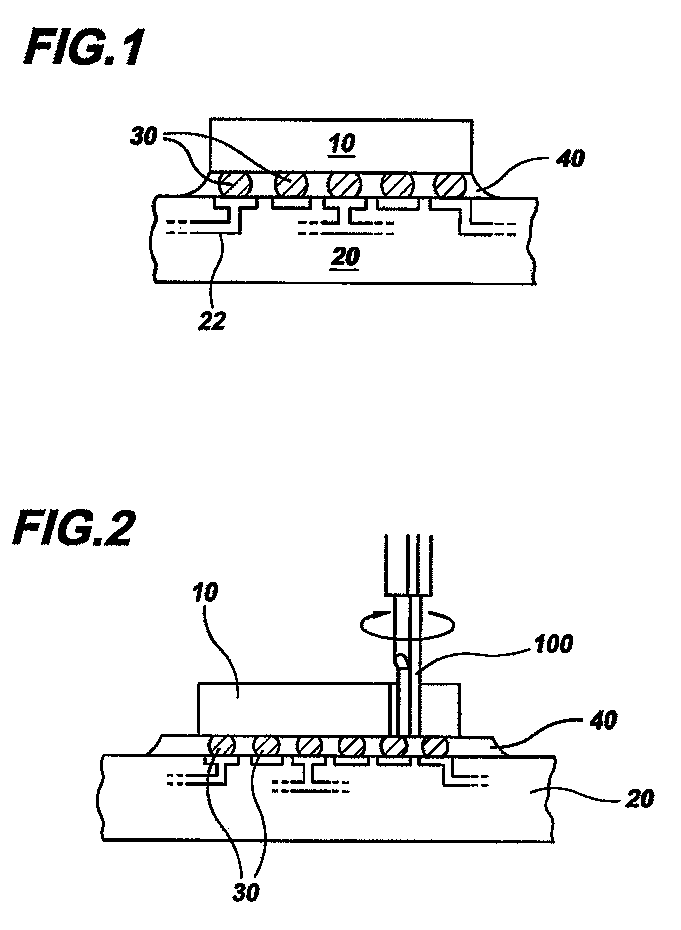
Figure 2 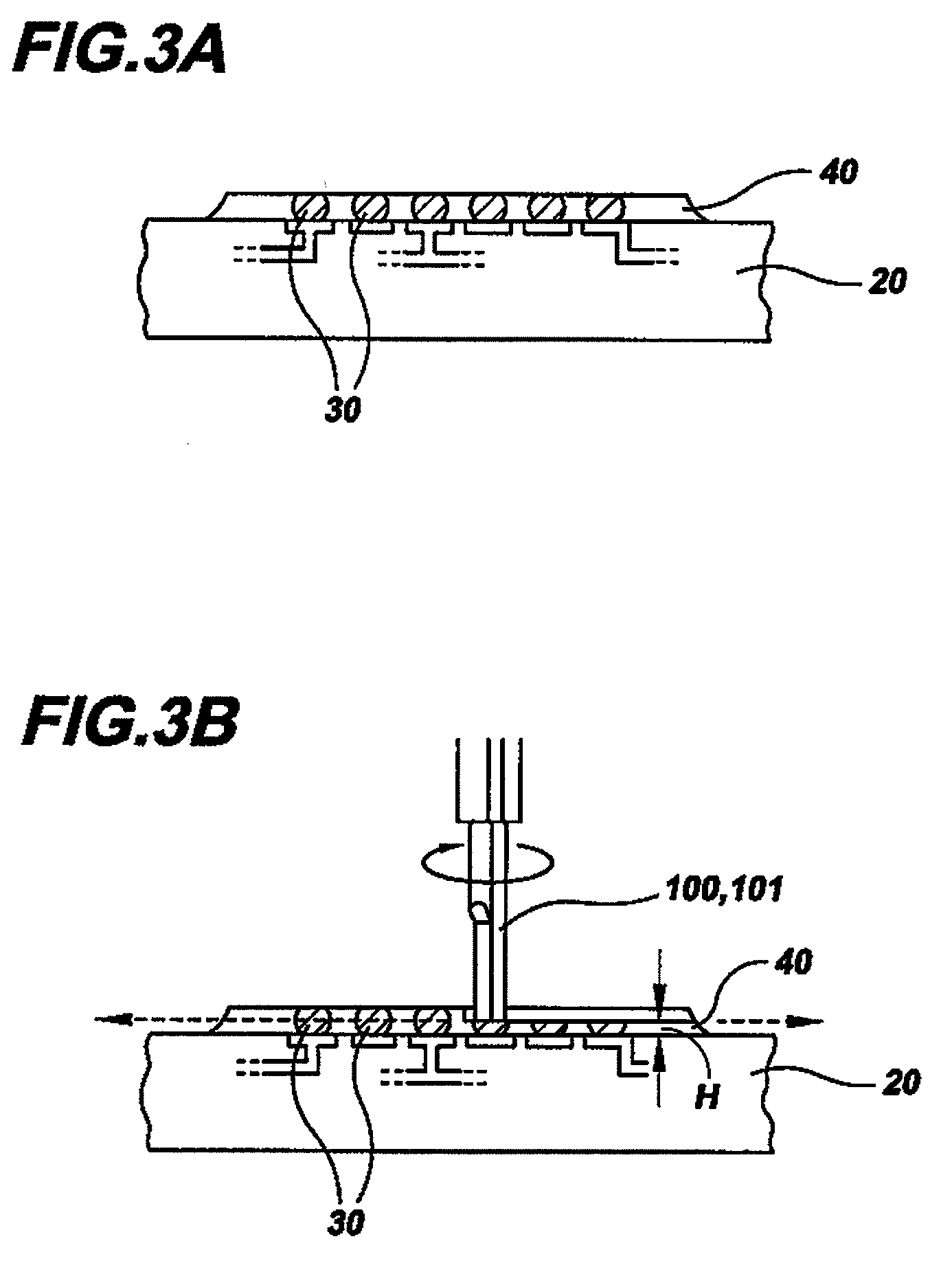
Figure 3
Abstract
Description
BACKGROUND OF THE INVENTION
[0001] 1. Field of the Invention
[0002] The present invention relates to electronic devices, and in particular, to removing and reworking underfilled integrated circuit chips on an electronic module.
[0003] 2. Description of Related Art
[0004] Electronic components include both Single Chip Modules (SCMs) and Multi Chip Modules (MCMs). While SCMs contain a single chip, MCMs contain numerous chips on a substrate, and as such, are key components for many high-end computer servers and mainframes.
[0005] Often, the electronic components in SCMs and MCMs are joined to other components by solder interconnections whereby these solder interconnections are made by soldering pads on a surface of a first of these electronic components to corresponding soldering pads on the surface of the second component. Typical solder surface mount processes involve screening solder paste onto exposed metallic pads of a board or substrate, followed by a thermal reflow to bring the solder int...
Examples
Embodiment Construction
)
[0039]In describing the preferred embodiment of the present invention, reference will be made herein to FIGS. 1-9C of the drawings in which like numerals refer to like features of the invention.
[0040]The material set and method disclosed herein are the basis for a low cost electronic package rework process including appropriate hardware and equipment alternatives. An advantage of the foregoing rework method and material set is that it can be implemented on many levels of scale at minimal cost, with minimal effort and ease of flexibility, as well as across a variety of differing types and material sets of electronic packages.
[0041]In accordance with the invention, an electronic package typically has many electrical components attached to a substrate using encapsulated solder connections. Referring to FIG. 1, for ease of understanding the invention, reference is made to the electronic device or component being removed from the module as a semiconductor chip or die 10 attached to a su...