
Liquid ejecting head, piezoelectric element, and liquid ejecting apparatus
a piezoelectric element and liquid ejecting technology, applied in printing and other directions, can solve the problem of low piezoelectric layer movement inhibition of protective film, and achieve the effect of increasing the displacement amount, preventing degradation, and increasing the area
Patent Information
- Authority / Receiving Office
- US · United States
- Patent Type
- Applications(United States)
- Current Assignee / Owner
- Publication Date
- 2009-10-01
Smart Images
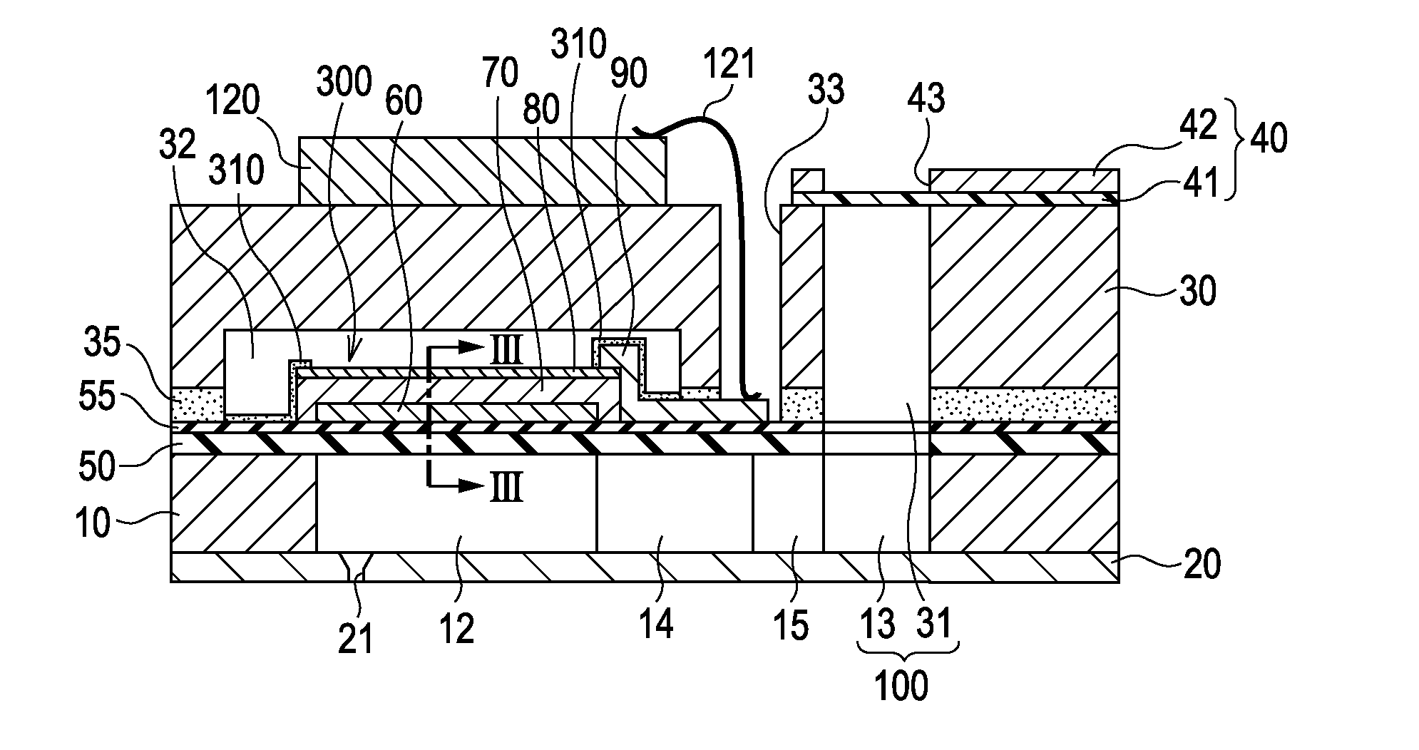
Figure 1 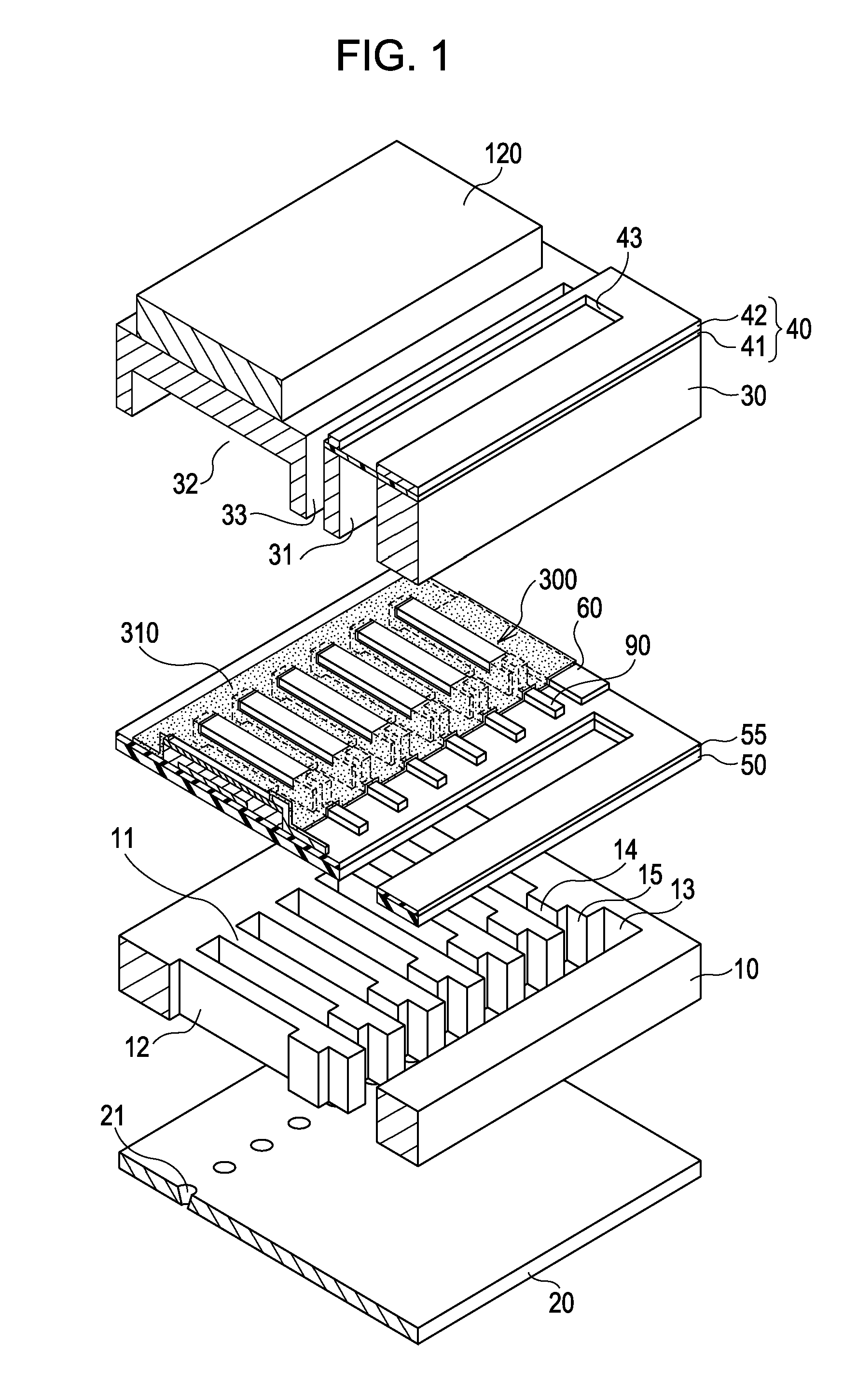
Figure 2 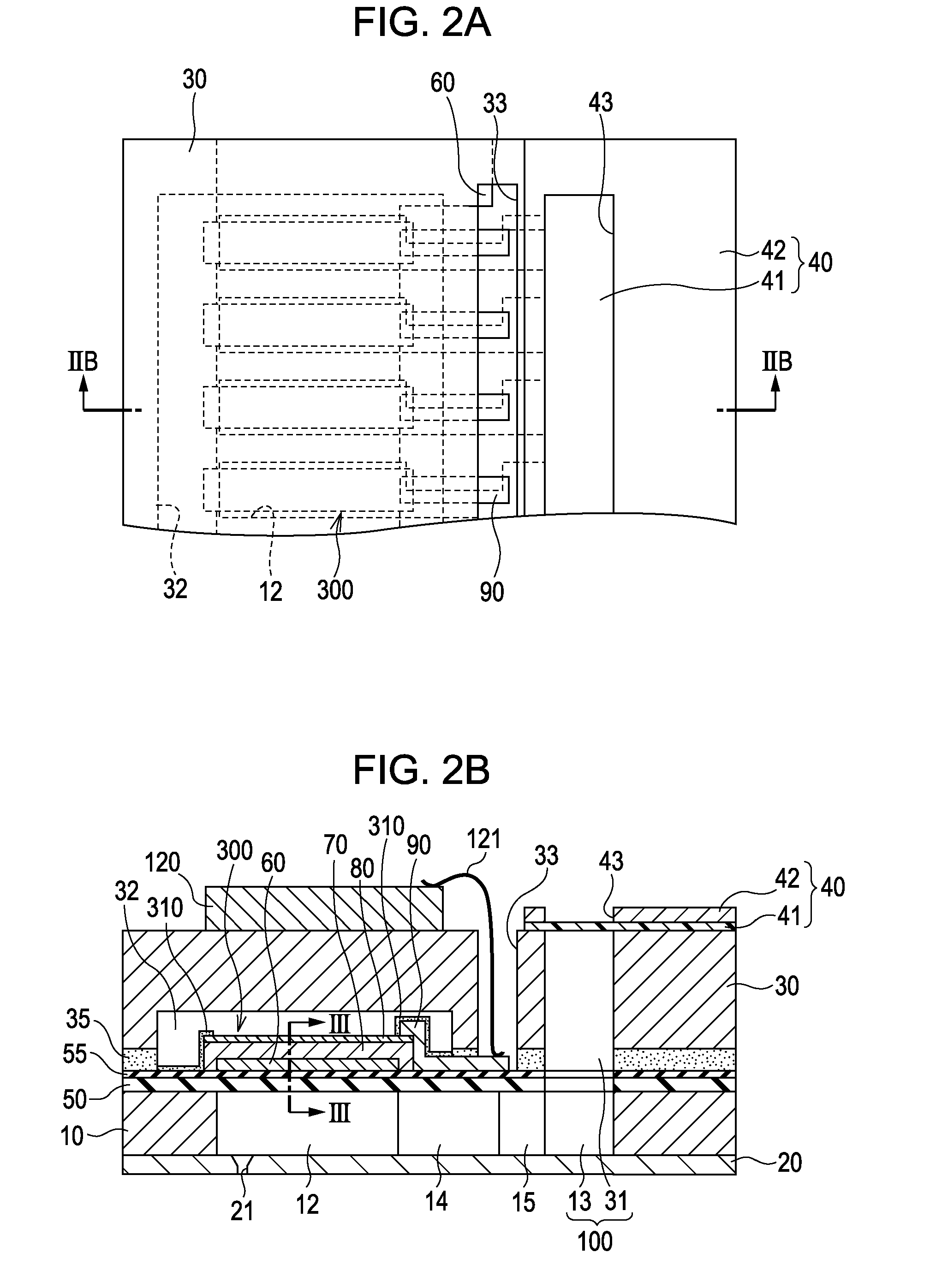
Figure 3
Abstract
Description
[0001] This application claims priority to Japanese Patent Application No. 2008-088176 filed on Mar. 28, 2008 and Japanese Patent Application No. 2009-002958, filed on Jan. 8, 2009, the entire disclosures of which are expressly incorporated by reference herein.BACKGROUND
[0002] 1. Technical Field
[0003] The present invention relates to a liquid ejecting head, a piezoelectric element, and a liquid ejecting apparatus.
[0004] 2. Related Art
[0005] As an example of a liquid ejecting head, an ink ejecting recording head in which a piezoelectric element consisting of an upper electrode, a piezoelectric layer, and a lower electrode is used as a pressure generating unit is known (reference should be made to, for example, claim 2 and FIG. 6 of JP-A-2000-246888). In such an ink ejecting recording head, an insulation layer for preventing moisture degradation of the piezoelectric layer is formed in a state of covering the piezoelectric layer and the upper electrode.
[0006] According to the above-mentioned...
Examples
Embodiment Construction
[0019]Exemplary embodiments will be described herein below with reference to the accompanying drawings. FIG. 1 is an exploded perspective view showing a simplified structure of an ink ejecting recording head which is an example of a liquid ejecting head according to the present embodiment. FIG. 2A is a top plan view of FIG. 1, and FIG. 2B is a sectional view taken along the line IIA-IIA′ in FIG. 2A. For better understanding of the drawing, a later-described protective film 310 is not depicted in FIG. 2A.
[0020]A flow path forming substrate 10 is formed of a single crystal silicon substrate which has a plane (110) of the plane orientation in the present embodiment. An elastic film 50 which is preliminarily formed of silicon dioxide by thermal oxidation is formed on one surface of the flow path forming substrate 10. An insulation film 55 formed of zirconium oxide (ZrO2) or the like is formed on the elastic film 50. On the other surface of the flow path forming substrate 10, pressure ge...