
Display device, method for driving the same, and electronic device using the display device and the method
Patent Information
- Authority / Receiving Office
- US · United States
- Current Assignee / Owner
- Publication Date
- 2010-06-10
- Estimated Expiration
- Not applicable · inactive patent
Smart Images
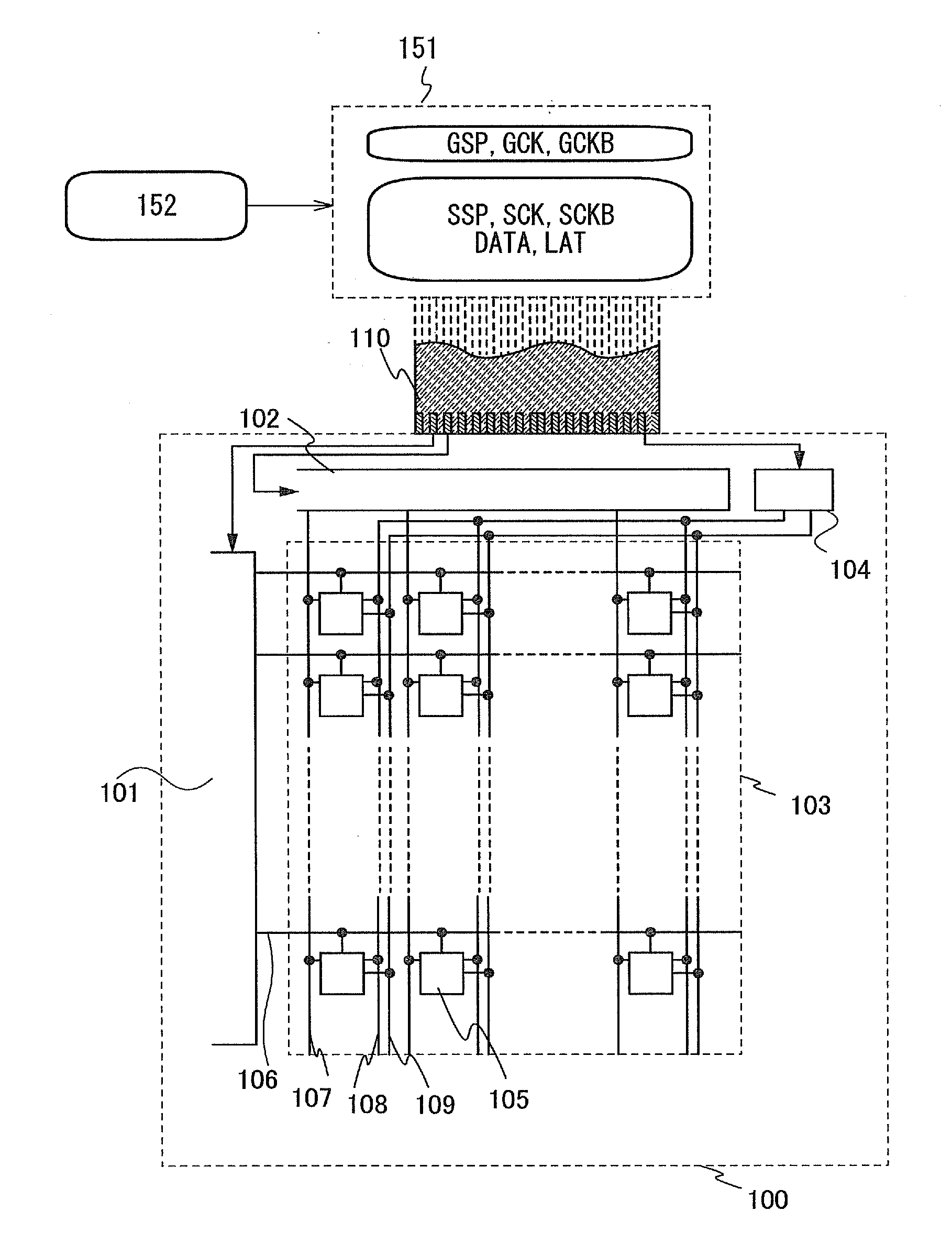
Figure 1 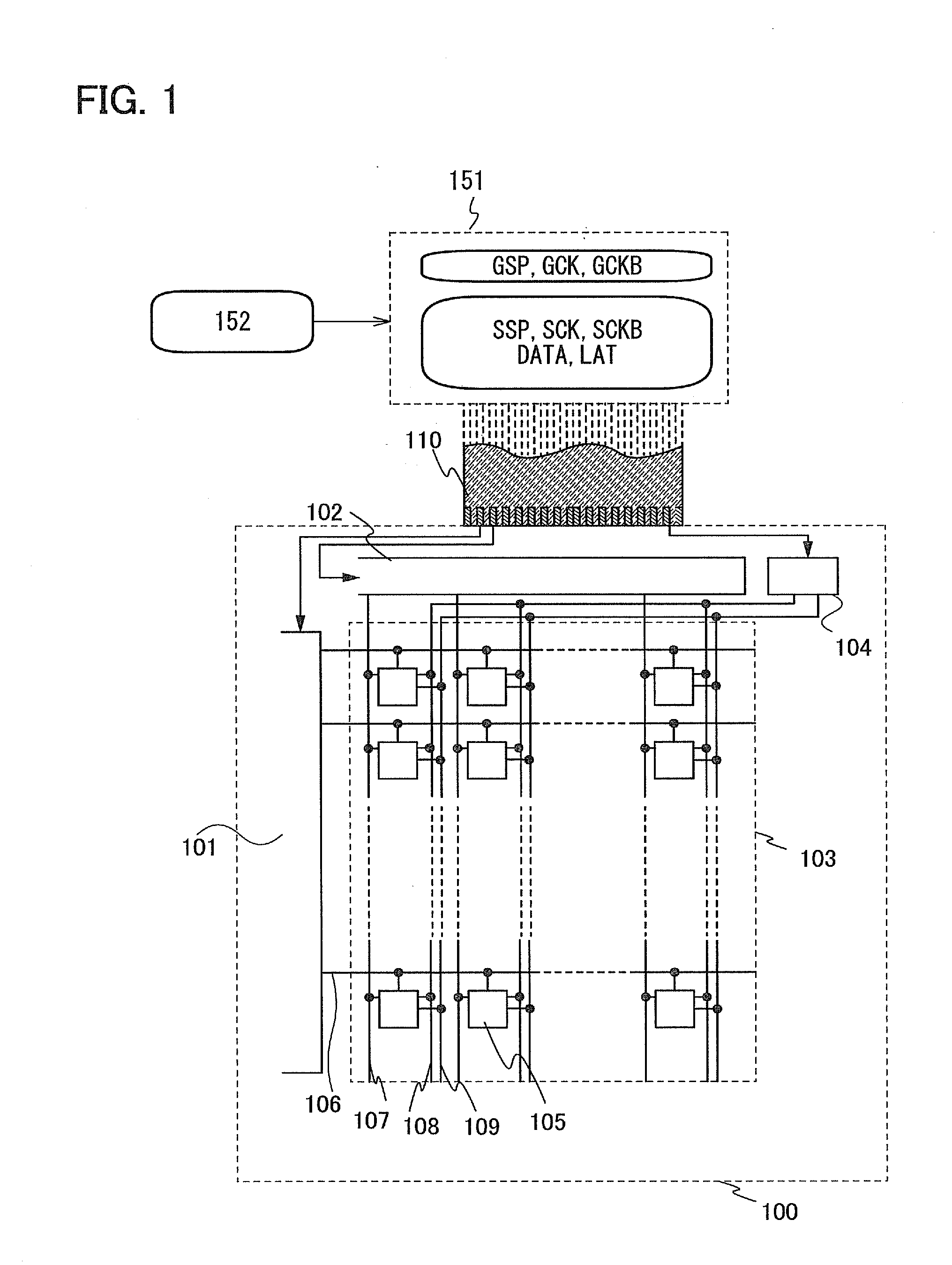
Figure 2 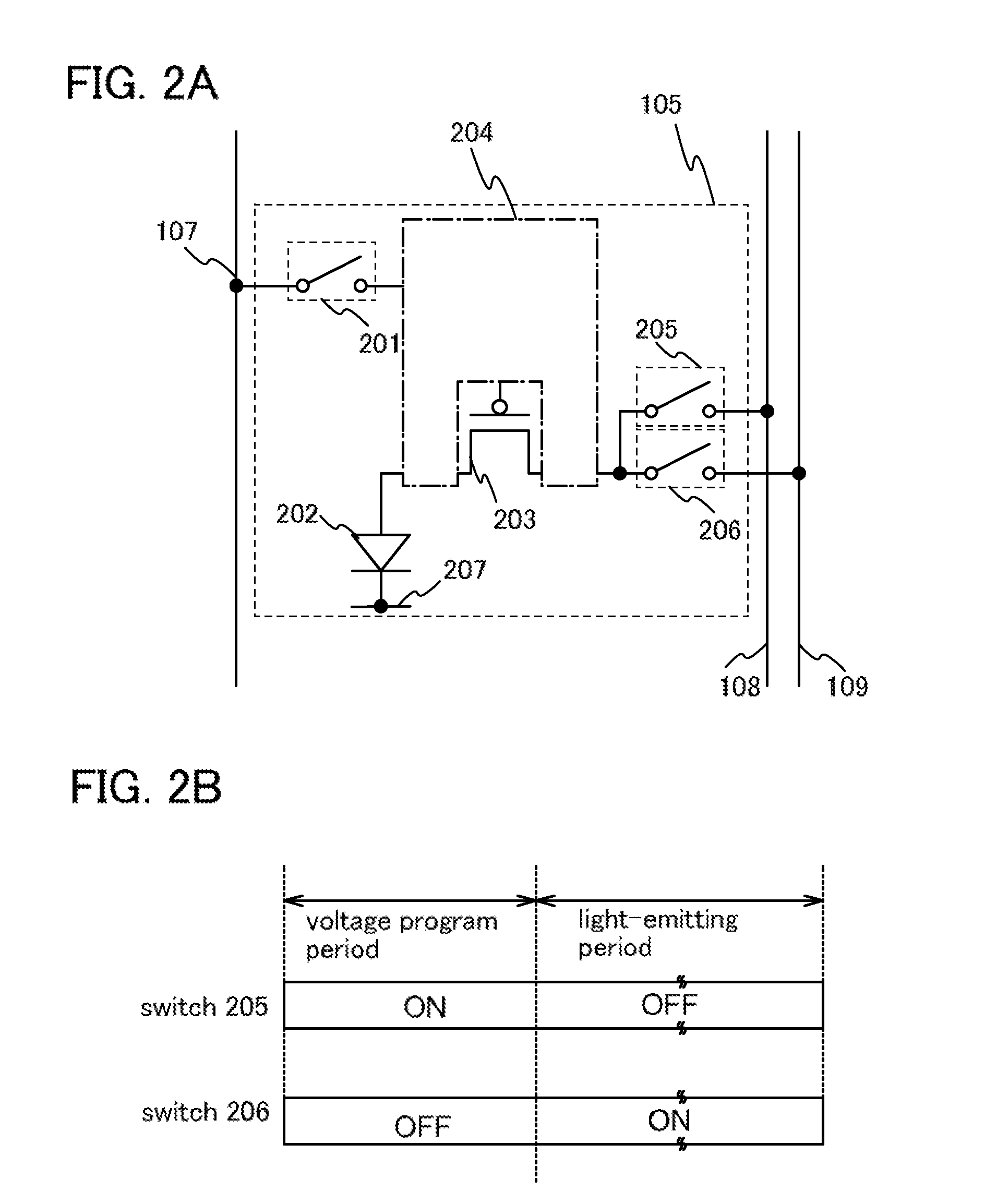
Figure 3
Abstract
Description
BACKGROUND OF THE INVENTION
[0001] 1. Field of the Invention
[0002] The present invention relates to a semiconductor device, a display device, and a light-emitting device, and a method for driving a semiconductor device, a display device, and a light-emitting device. Further, the present invention relates to an electronic device including the semiconductor device, the display device, or the light-emitting device.
[0003] 2. Description of the Related Art
[0004] Display devices are used for a variety of electric products such as a mobile phone and a television receiver. As a display element used in a display device, a light-emitting element such as an EL element (an EL element containing an organic material and an inorganic material, an organic EL element, and an inorganic EL element) is favorable for improving the image quality because of high contrast ratio, high response speed to input signals, and wide viewing angle characteristics, and thus has been actively researched. Moreover, as for ...
Examples
embodiment 1
[0046]First, a block diagram of a display device for illustrating a structure in this embodiment will be described.
[0047]FIG. 1 illustrates a structure of a gate line driver circuit 101, a signal line driver circuit 102, a display portion 103, and a power supply circuit 104 which are included in a display device 100. In the display portion 103, a plurality of pixels 105 are arranged in matrix. FIG. 1 also illustrates a signal generation circuit 151 for generating a signal input to the display device.
[0048]In FIG. 1, the gate line driver circuit 101 supplies scan signals to a plurality of wirings 106. By these scan signals, the pixels 105 are determined to be in a selected state or a non-selected state per row. The signal line driver circuit 102 supplies a video voltage (also referred to as a video signal or video data) from a wiring 107 to the pixel 105 selected by the scan signal. The power supply circuit 104 generates a first potential supplied to a wiring 108 (also referred to as...
embodiment 2
[0161]In this embodiment, a structure of a display panel having a display portion including a variety of pixel circuits described in Embodiment 1 will be described.
[0162]Note that in this embodiment, a display panel includes a substrate where a pixel circuit is formed and the whole structure which is formed in contact with the substrate. For example, when a pixel circuit is formed over a glass substrate, a glass substrate, a transistor formed in contact with the glass substrate, a wiring, and the like are collectively referred to as a display panel.
[0163]A display panel is sometimes provided with a peripheral driver circuit for driving a pixel circuit in addition to a pixel circuit (integrated formation). A peripheral driver circuit typically includes, in its category, a scan driver for controlling a scan line of a display portion (also referred to as a scan line driver, a gate driver, or the like) and a data driver for controlling a signal line (also referred to as a signal line dr...
embodiment 3
[0187]In this embodiment, a structure and a manufacturing method of a transistor will be described.
[0188]FIGS. 12A to 12G illustrate examples of structures and a manufacturing method of transistors. FIG. 12A illustrates examples of structures of transistors. FIGS. 12B to 12G illustrate an example of a method for manufacturing transistors.
[0189]Note that the structure and the manufacturing method of transistors are not limited to those illustrated in FIGS. 12A to 12G, and a variety of structures and manufacturing methods can be used.
[0190]First, structure examples of transistors are described with reference to FIG. 12A. FIG. 12A is a cross-sectional view of a plurality of transistors each having a different structure. Here, in FIG. 12A, the plurality of transistors each having different structures are placed in a line, which is for describing structures of the transistors. Accordingly, the transistors are not needed to be actually placed as illustrated in FIG. 12A and can be separate...