
Method for Semiconductor Leadframes in Low Volume and Rapid Turnaround
a leadframe and low-volume technology, applied in semiconductor devices, semiconductor/solid-state device details, electrical equipment, etc., can solve the problems of affecting the reliability of devices, wasting time and investment money, and presently taking too much cycle time and investment money to tool up stamping machines, photomasks, etching baths, etc., to achieve strong adhesion between leadframe and polymeric encapsulation, reduce cycle time, and easy to oxidize
Patent Information
- Authority / Receiving Office
- US · United States
- Patent Type
- Applications(United States)
- Current Assignee / Owner
- Publication Date
- 2010-11-25
Smart Images
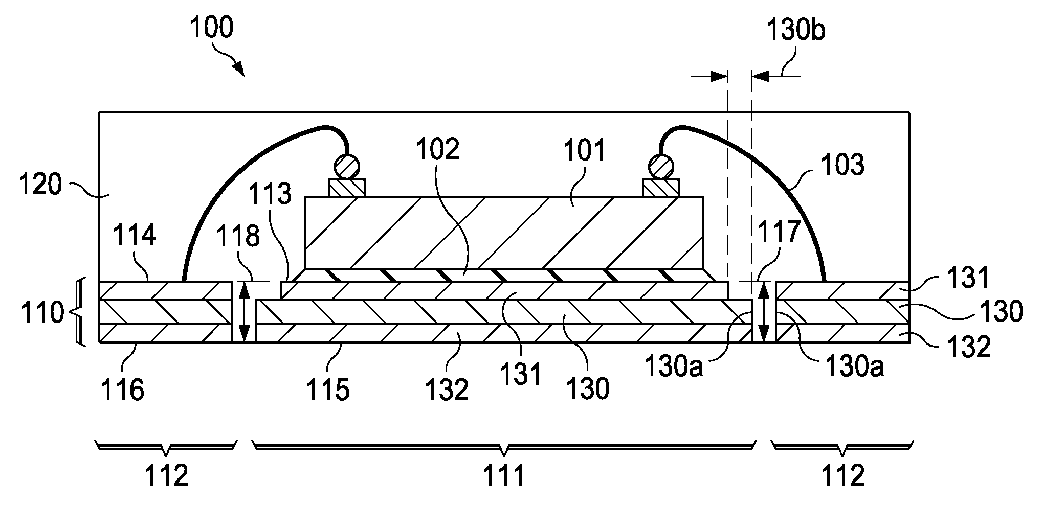
Figure 1 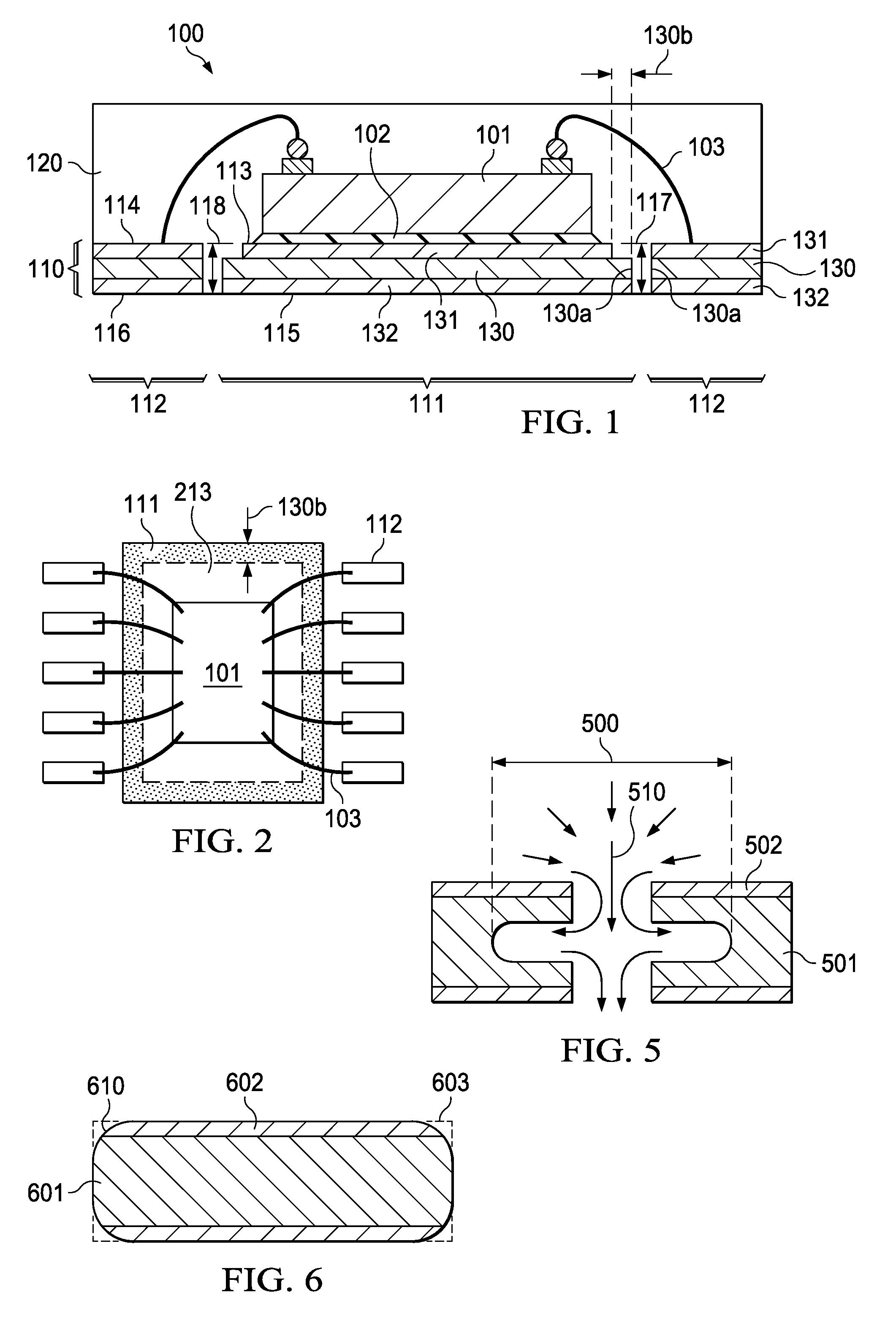
Figure 2 
Figure 3
Abstract
Description
FIELD OF THE INVENTION
[0001] The present invention is related in general to the field of semiconductor devices and processes, and more specifically to the structure and fabrication method of semiconductor leadframes for low volume, yet high diversity Quad Flat No-Lead (QFN) and Small Outline No-Lead (SON) devices.DESCRIPTION OF RELATED ART
[0002] The metallic leadframes used in semiconductor devices such as dual-in-line devices, surface mount devices, and Quad Flat No-Lead (QFN) and Small Outline No-Lead SON) devices, provide a pad for stable support of the semiconductor chip, and a plurality of leads to bring electrical conductors in close proximity of the chip. After attaching the chip onto the pad, the remaining gap between the chip and a lead is usually bridged by a thin wire attached in a bonding process; the wires are typically made of gold or copper. In order to protect the sensitive chip and wires from environmental disturbances such as moisture, scratches and light, the assemb...
Examples
Embodiment Construction
[0021]FIG. 1 depicts an exemplary semiconductor device of the Quad Flat No-Lead (QFN), or Small Outline No-Lead (SON) type, generally designated 100, as an embodiment of the invention. A semiconductor chip 101 is attached by a polymeric material 102 to the pad 111 of a metallic leadframe 110. Besides pad 111, the leadframe 110 has a plurality of leads 112. Pad 111 has a first surface 113 and a second surface 115, which is parallel to first surface 113. Leads 112 have a first surface 114 and a second surface 116, which is parallel to first surface 114. In FIG. 1, first surface 113 of the pad and first surface 114 of the leads lie in one plane, and second surface 115 of the pad and second surface 116 of the leads lie in another parallel plane. In other semiconductor devices, pad 111 and leads 112 may be offset relative to each other so that the pad first surface is in a plane different from but parallel to the plane of the lead first surfaces.
[0022]Pad 111 further has sidewalls 117 or...