
Semiconductor Structure and Method for Manufacturing the Same
a technology of semiconductors and semiconductors, applied in the direction of semiconductor devices, electrical devices, transistors, etc., can solve the problems of short channel effects, and achieve the effects of reducing parasitic capacitance, parasitic capacitance reduction, and contact resistance reduction of the source extension region
Patent Information
- Authority / Receiving Office
- US · United States
- Patent Type
- Applications(United States)
- Current Assignee / Owner
- Publication Date
- 2012-09-20
- Estimated Expiration
- Not applicable · inactive patent
Smart Images
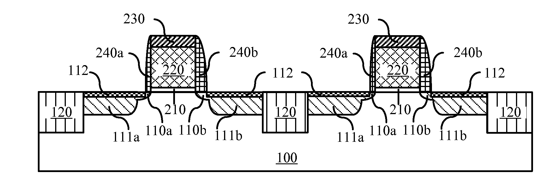
Figure 1 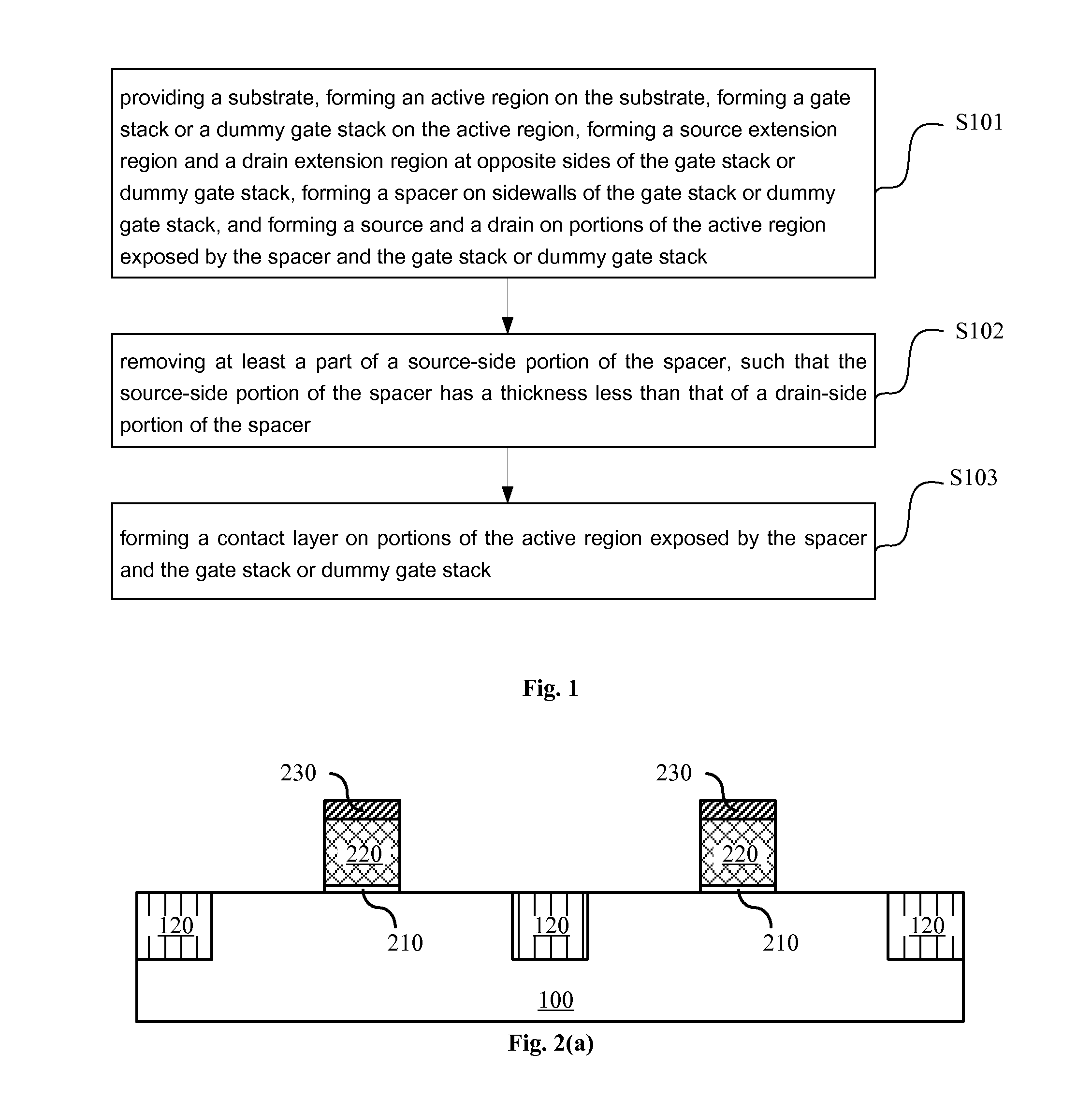
Figure 2 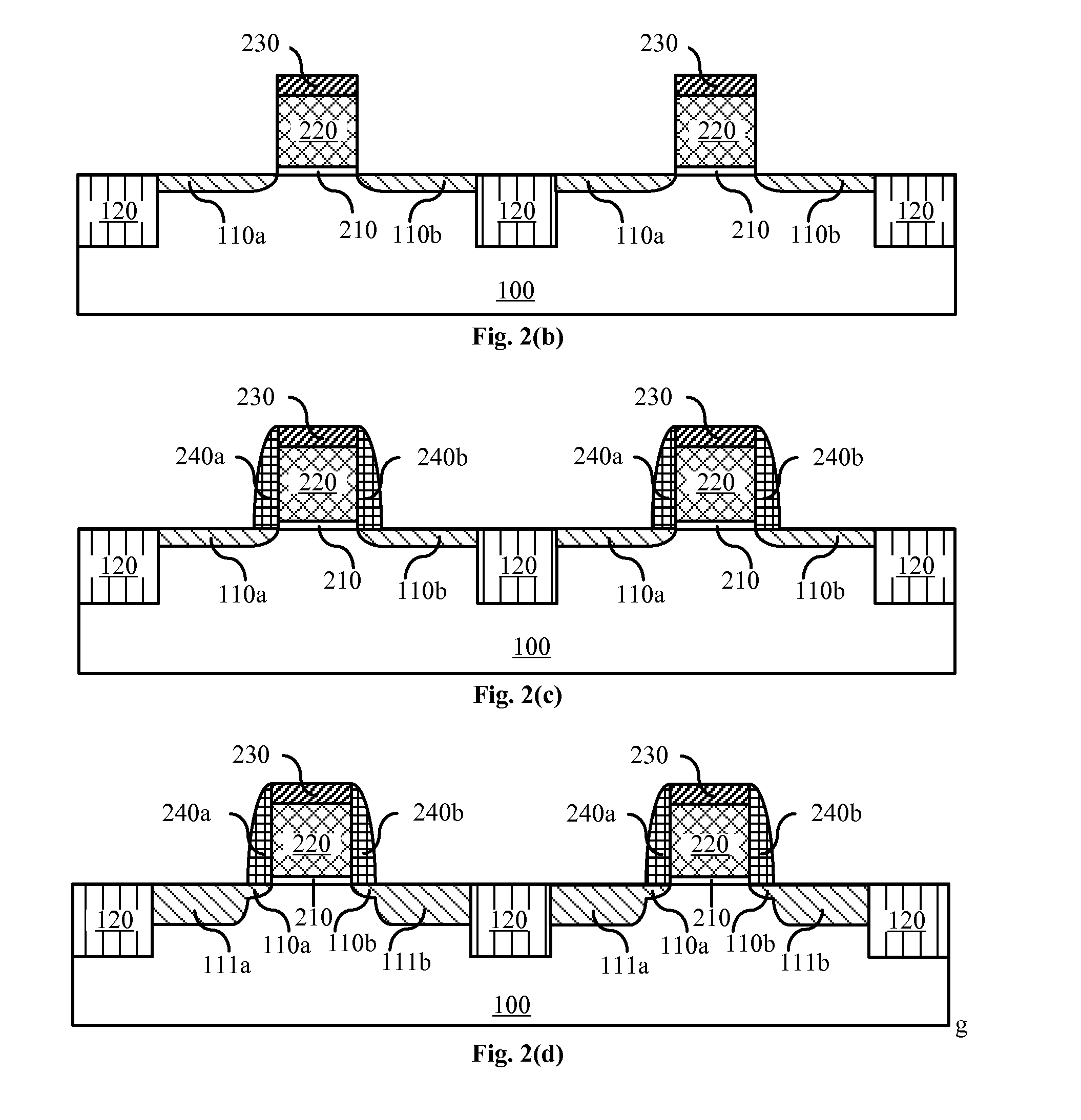
Figure 3
Abstract
Description
[0001] This application claims priority to a Chinese Patent Application No. 201110066929.0, filed on Mar. 18, 2011 and entitled “SEMICONDUCTOR STRUCTURE AND METHOD FOR MANUFACTURING THE SAME”, which is hereby incorporated by reference in its entirety.FIELD OF THE INVENTION
[0002] The present invention relates to the semiconductor manufacturing technology, and particularly to a semiconductor structure and a method for manufacturing the same.BACKGROUND OF THE INVENTION
[0003] A metal-oxide-semiconductor field-effect transistor (MOSFET) is a transistor that can be widely used in digital circuits and analog circuits. With continuous reduction in a size of the semiconductor structure, a length of a channel beneath a gate decreases correspondingly, thereby causing occurrence of short channel effects. A common means for reducing short channel effects is to form a source extension region and a drain extension region with a shallow depth.
[0004] In order to improve the performance of the semiconduc...
Examples
Embodiment Construction
[0036]The embodiments of the present invention are described in detail as follows, the examples of which are shown in the drawings. The embodiments described as follows in reference to the drawings are exemplary and merely used to interpret the present invention, instead of restricting the present invention.
[0037]The following disclosure provides many different embodiments or examples for implementing different structures of the present invention. In order to simplify the disclosure of the present invention, the components and arrangement of specific examples are described in the following text. Apparently, they are just exemplary, and do not intend to restrict the present invention. In addition, reference numbers and / or letters can be repeatedly used in different examples of the present invention for the purposes of simplification and clearness, without indicating the relationships between the discussed embodiments and / or arrangements. Furthermore, the present invention provides ex...