
Multi-spot scanning device, system and method
Patent Information
- Authority / Receiving Office
- US · United States
- Current Assignee / Owner
- Publication Date
- 2021-08-05
Smart Images
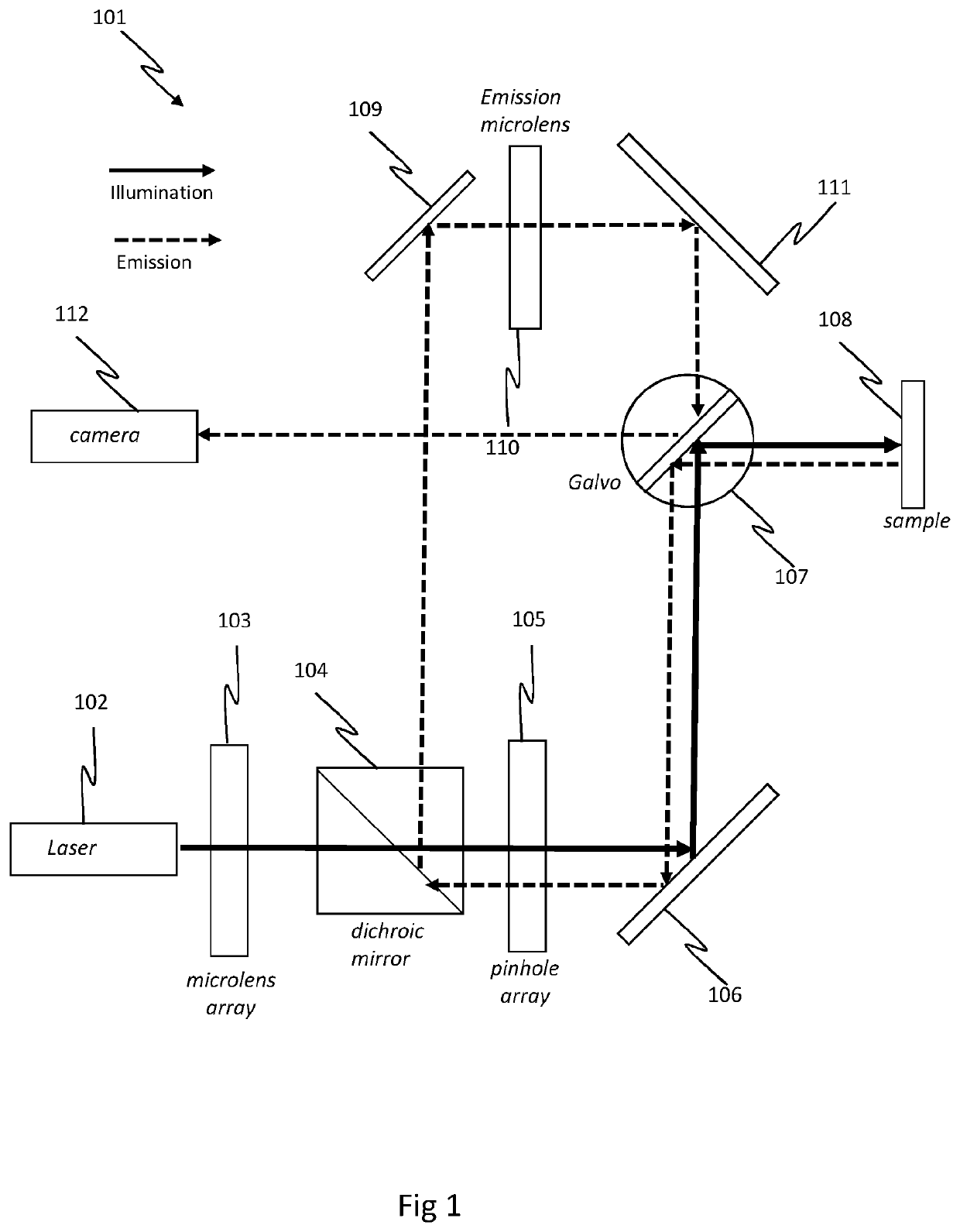
Figure 1 
Figure 2 
Figure 3
Abstract
Description
TECHNICAL FIELD
[0001] The present invention relates to an improved confocal scanning, device, system and method.BACKGROUND
[0002] Confocal imaging systems are well known and widely used. Advanced multi-point confocal scanning systems use a technique in which an array of illumination beams is scanned across a sample plane usually by virtue of a galvanometer mirror, piezo mirror or spinning “Nipkow” disk. A corresponding array of emission beams are stimulated (typically through fluorescence) from the sample which are passed through a pinhole array with the same architecture as the illumination beams. This removes any out of focus light so that when the emission beams are scanned or relayed onto a sensor of an imaging device, a focussed image is produced.
[0003] Such systems enable very high temporal and spatial resolution to be achieved. Each illumination beam incident on the sample surface and corresponding emission beam incident on the imaging plane can be modelled as a point spread func...
Examples
Embodiment Construction
[0038]FIG. 1 provides a simplified schematic diagram of a conventional confocal scanning system 101.
[0039]The system comprises a laser light source 102, a two-dimensional microlens array 103, a dichroic mirror 104, a two-dimensional confocal pinhole array 105, a first mirror 106, a galvanometer mirror 107 and a sample stage on which is mounted a sample 108 (target surface). The system further comprises a second mirror 109, an emission microlens 110, a third mirror 111 and an imaging camera 112. As will be understood, a typical confocal scanning system will comprise further components, such as relay optics, however, for clarity such components are omitted from FIG. 1.
[0040]The system shown in FIG. 1 is sometimes referred to as a “super-resolution” imaging system by virtue of the provision of the emission microlens 110 (described in more detail below). Certain systems are provided without the emission microlens 110, but the operating principle is the same.
[0041]In use, collimated lase...