
Device and Method for Measuring Thickness of Dielectric Layer in Circuit Board
a dielectric layer and circuit board technology, applied in the direction of electrical/magnetic thickness measurement, printed circuit testing, instruments, etc., can solve the problems of circuit board scrapping, high cost, time-consuming and laborious prior art, etc., and achieve the effect of quick and easy measurement of the thickness of the dielectric layer
Patent Information
- Authority / Receiving Office
- US · United States
- Patent Type
- Applications(United States)
- Current Assignee / Owner
- Publication Date
- 2022-07-14
Smart Images
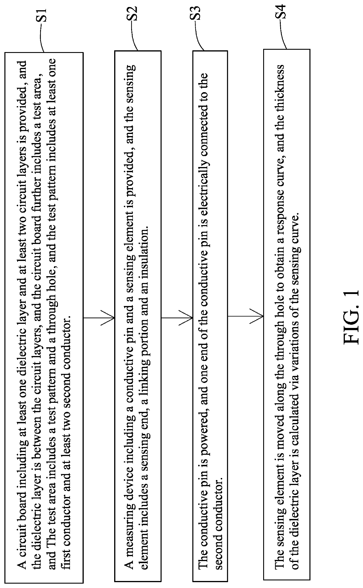
Figure 1 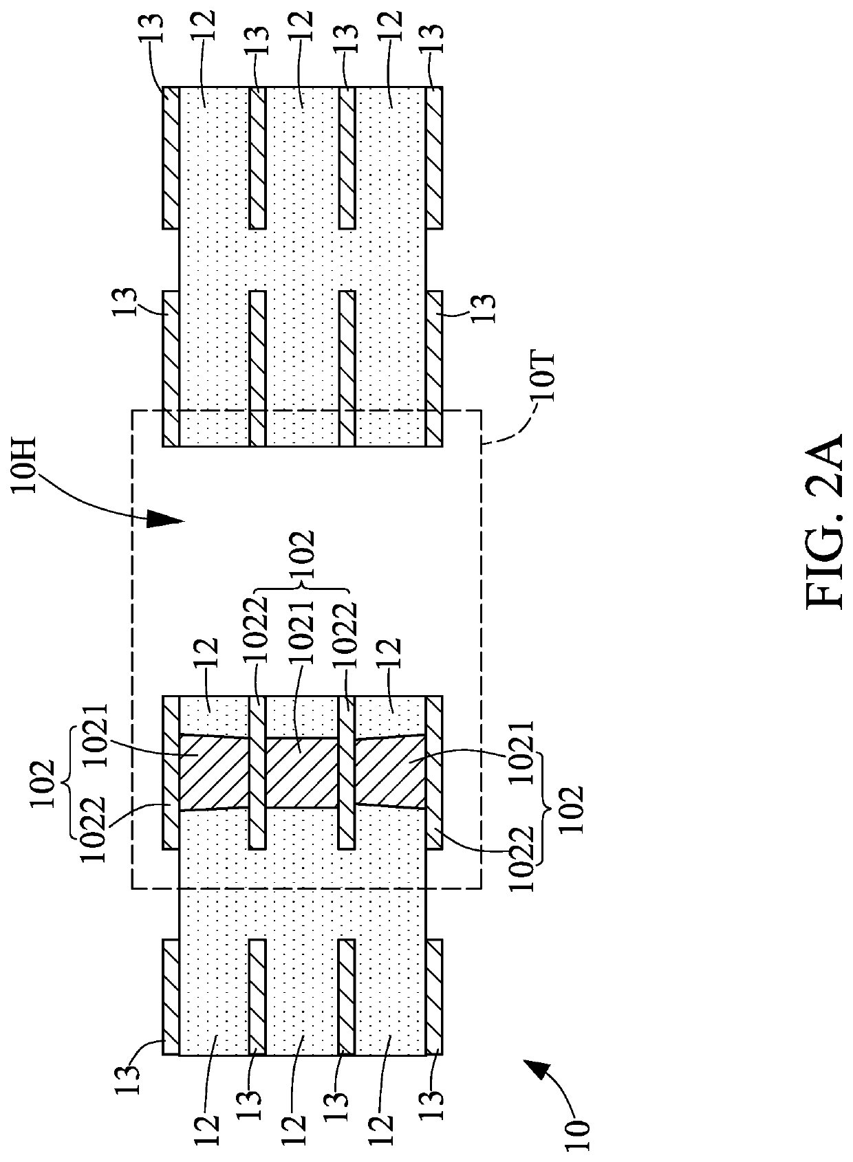
Figure 2 
Figure 3
Abstract
Description
FIELD OF THE DISCLOSURE
[0001] The present invention relates to a device and a method for measuring a thickness of a dielectric layer in a circuit board, and more particularly to the device and the method for measuring the thickness of the dielectric layer in the circuit board using a sensing element.BACKGROUND OF THE INVENTION
[0002] Currently, the thickness of the dielectric layer of the circuit board is mainly measured by destructive methods. For example, partial circuit board must be removed to be a measuring slice, firstly. Next, using optical microscope or scanning electron microscope is to measure the thickness. However, such prior art is very time-consuming and labor-intensive, and it will also damage a larger area of the circuit board and cause the circuit board to be scrapped.
[0003] Therefore, how to measure the thickness of the dielectric layer in the circuit board quickly and easily is worth considering for person having ordinary skill in the art.SUMMARY OF THE INVENTION[0004...
Examples
Embodiment Construction
[0025]Please refer to FIG. 1., which illustrates a schematic diagram of a method for measuring a thickness of a dielectric layer in a circuit board of the present invention. The method for measuring the thickness of the dielectric layer includes the following steps.
[0026]First, please refer to the step S1 and FIG. 2A. FIG. 2A illustrates a schematic partial cross-sectional view of a circuit board 10 of the present invention. The circuit board 10, including three dielectric layers 12 and four circuit layers 13, is provided. However, a person having ordinary skill in the art should understand that in practice, the circuit board 10 have more of the dielectric layers 12 and the circuit layers 13, or the circuit board 10 may only have one dielectric layer 12 and two circuit layers 13. The dielectric layer 12 is between the two circuit layers 13. In addition, the circuit board 10 further has a test area 10T having a test pattern 102 and a through hole 10H. The test pattern 102 has at leas...