
Method of inter-field critical dimension control
a critical dimension control and inter-field technology, applied in the direction of semiconductor/solid-state device testing/measurement, instruments, photomechanical equipment, etc., can solve the problems of reducing the stability of semiconductor chips obtained by dies, differences among manufacturing devices, and affecting the critical dimension control in the wafer manufacturing process. , to achieve the effect of simple and effectiv
Patent Information
- Authority / Receiving Office
- US · United States
- Patent Type
- Patents(United States)
- Current Assignee / Owner
- Publication Date
- 2005-04-05
- Estimated Expiration
- Not applicable · inactive patent
Smart Images
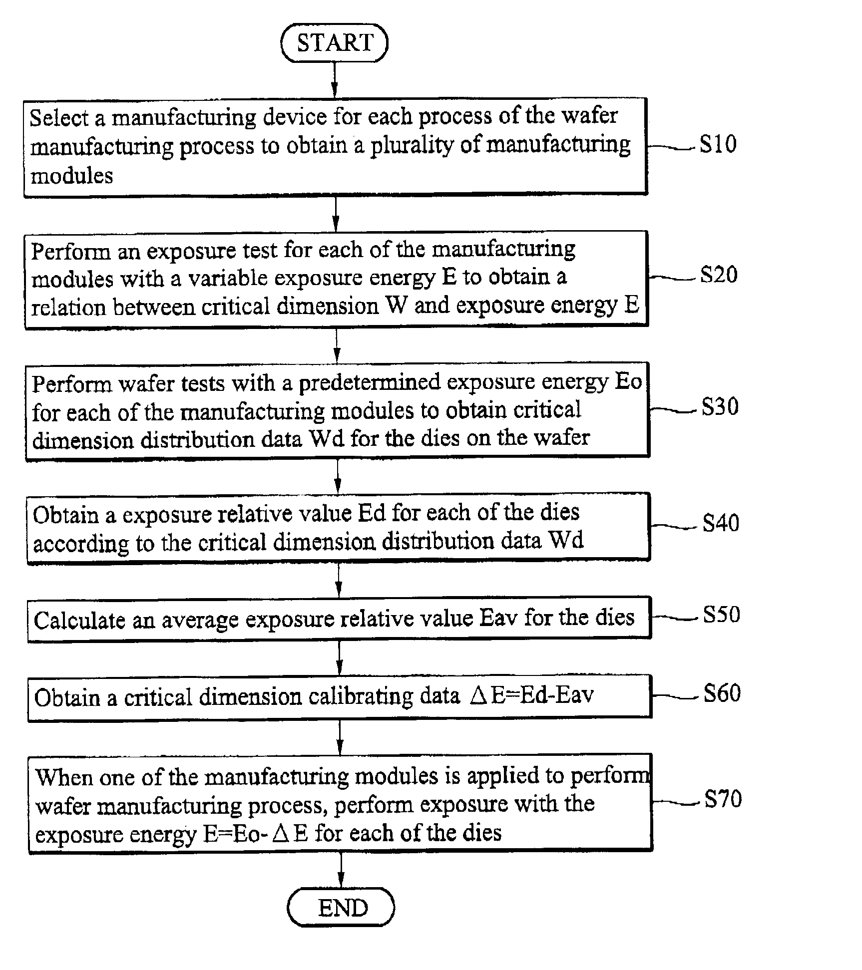
Figure 1 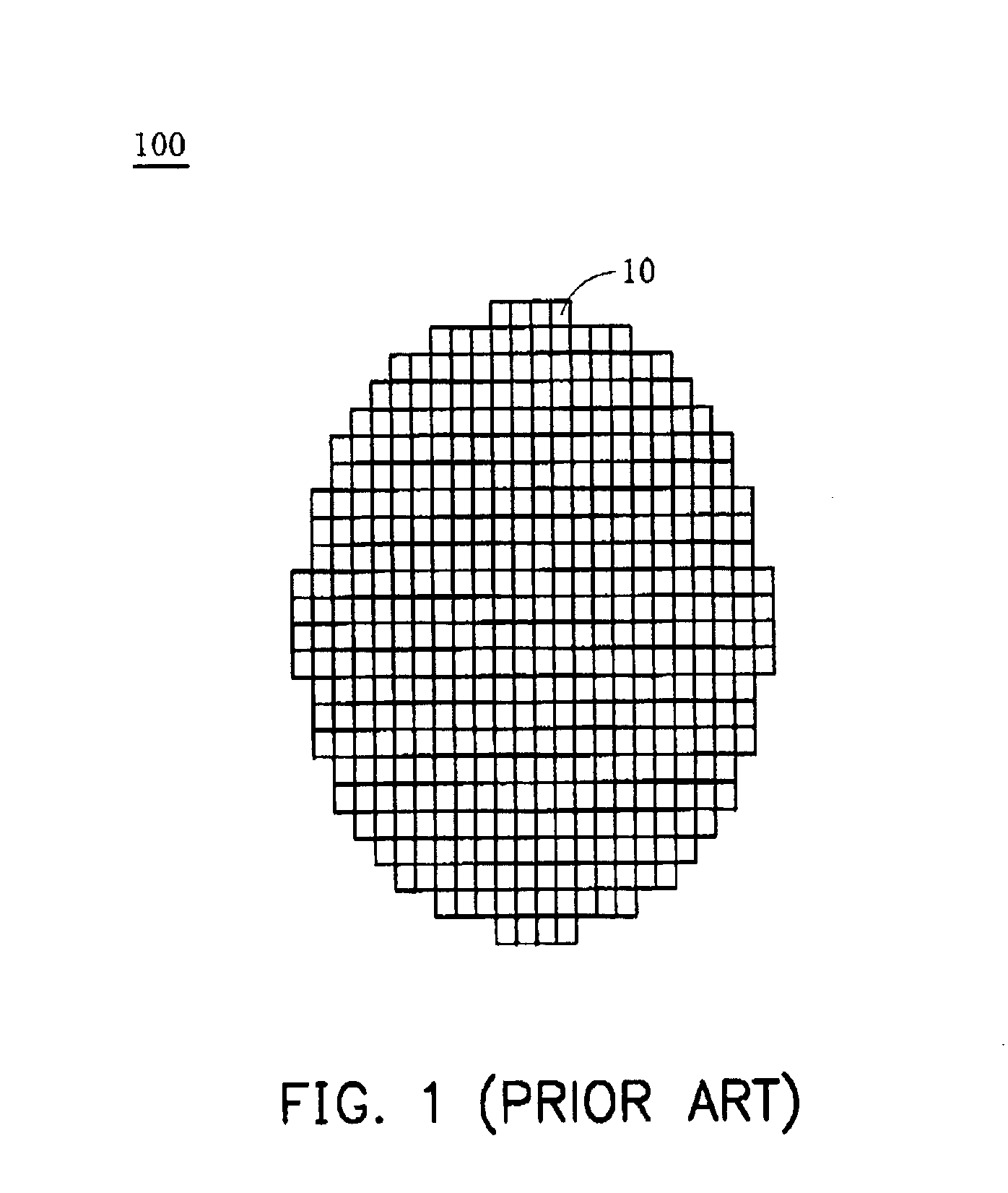
Figure 2 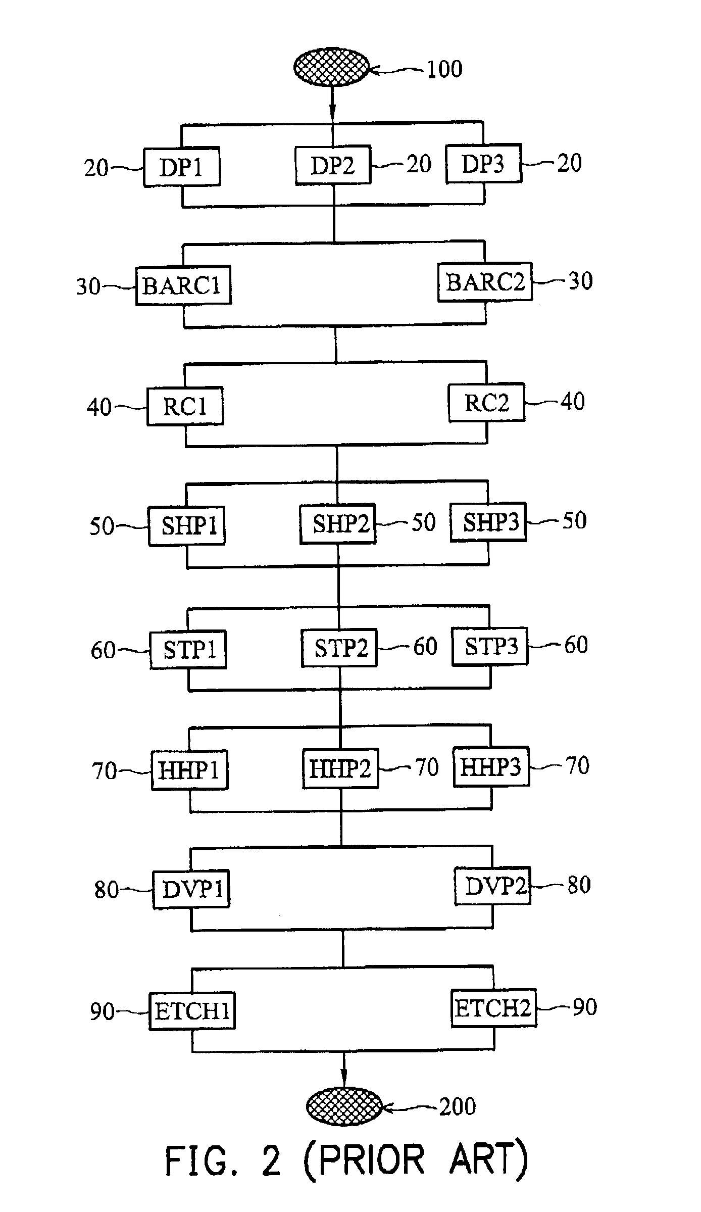
Figure 3
Abstract
Description
BACKGROUND OF THE INVENTION1. Field of the InventionThe present invention relates to a method of critical dimension control, and particularly to a method of inter-field critical dimension control for a wafer in semiconductor technique.2. Description of the Related ArtA critical dimension (CD) of a circuit is commonly defined as the smallest width of a line or the smallest space between two lines. Generally, the critical dimension is an important factor for the wafer manufacturing process. FIG. 1 shows a scheme of a wafer 100, which has a plurality of dies (or fields) 10. Generally, control of the critical dimension of the wafer 100 includes intra-field CD control and inter-field (or die-to-die) CD control. The intra-field CD control refers to control of the critical dimension in a individual die 10, so that the line width in the individual die 10 has approximately the same value. Meanwhile, the inter-field CD control refers to control of the critical dimension between the dies 10, s...
Examples
Embodiment Construction
The method of inter-field critical dimension control of the present invention can be hereinafter described with reference to FIG. 3. The method of inter-field critical dimension control of the present invention is applied to a wafer with a plurality of dies. The wafer manufacturing process has an exposure process.
First, before an experiment for the wafer manufacturing process begins, it is necessary to select a manufacturing device for each process of the wafer manufacturing process to obtain a plurality of manufacturing modules (step S10), such as the 1296 manufacturing modules in FIG. 2. It should be noted that in practical industrial application, not all of the 1296 manufacturing modules are generally applied in the wafer manufacturing process. In some cases, it is possible that only one of the manufacturing modules, such as a manufacturing module shown as DP1-BARC1-RC1-SHP1-STP1-HHP1-DVP1-ETCH1 in FIG. 2, is applied to perform all the wafer manufacturing process. Consequently, t...