
Localized radio frequency communication using asynchronous transfer mode protocol
a technology of asynchronous transfer and local radio frequency communication, applied in the field of wireless communication, can solve the problems of limiting the flexibility of a given circuit board design, redesigning and manufacturing a new circuit board, and high cost and time consumption, and achieves high pin density, noise-free connection, and high speed.
Patent Information
- Authority / Receiving Office
- US · United States
- Patent Type
- Patents(United States)
- Current Assignee / Owner
- Publication Date
- 2007-08-14
- Estimated Expiration
- Not applicable · inactive patent
Smart Images
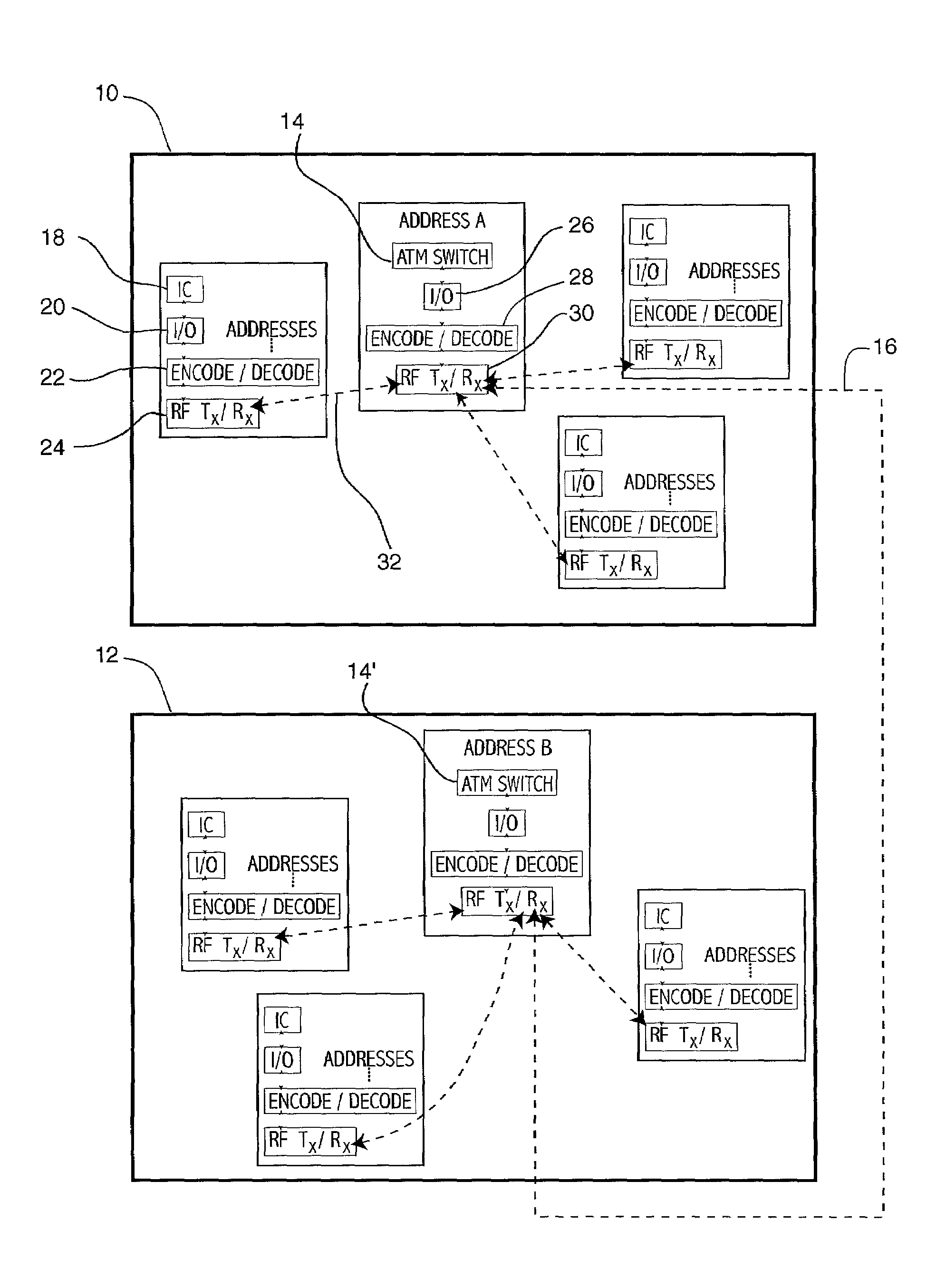
Figure 1 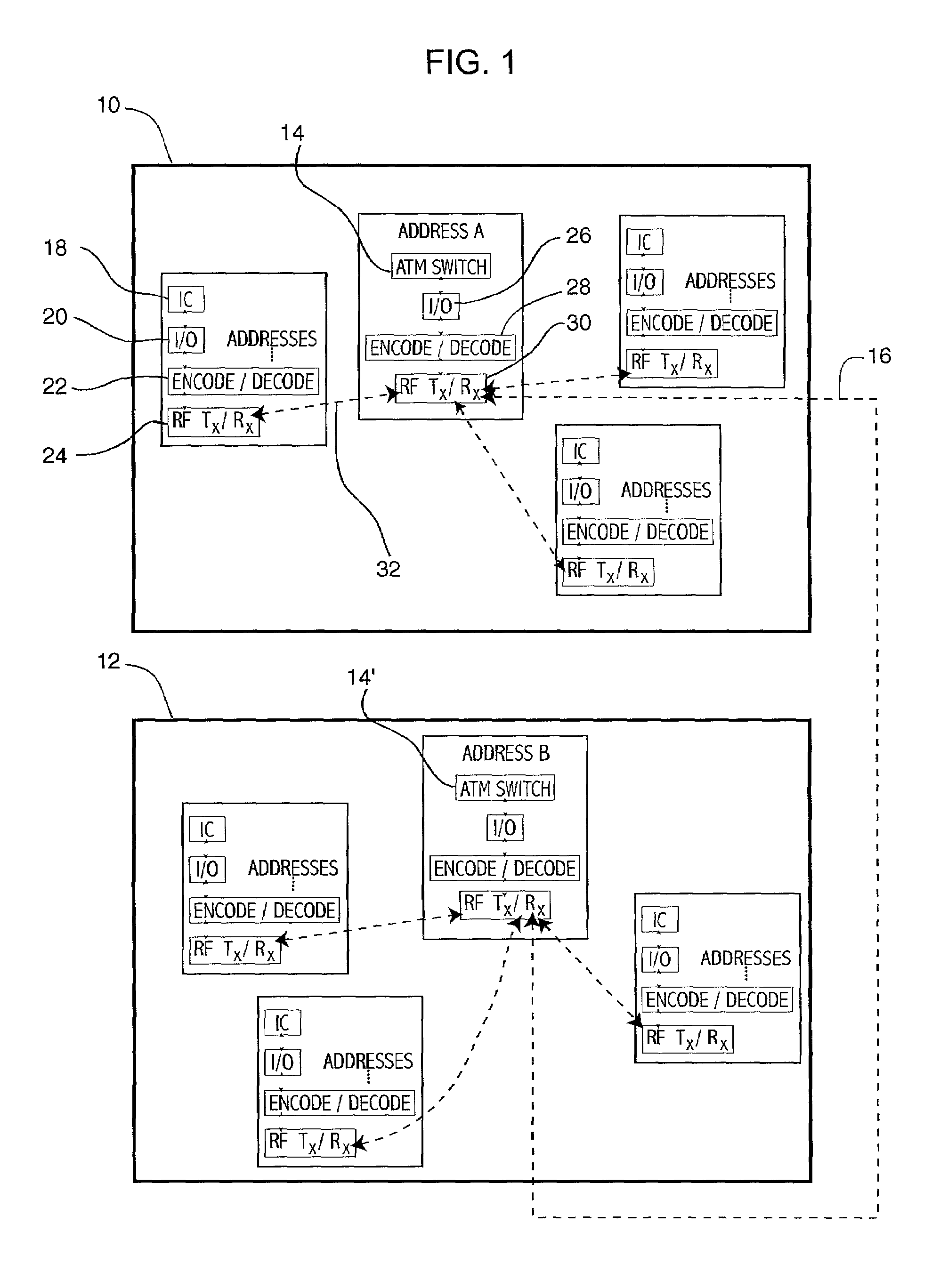
Figure 2 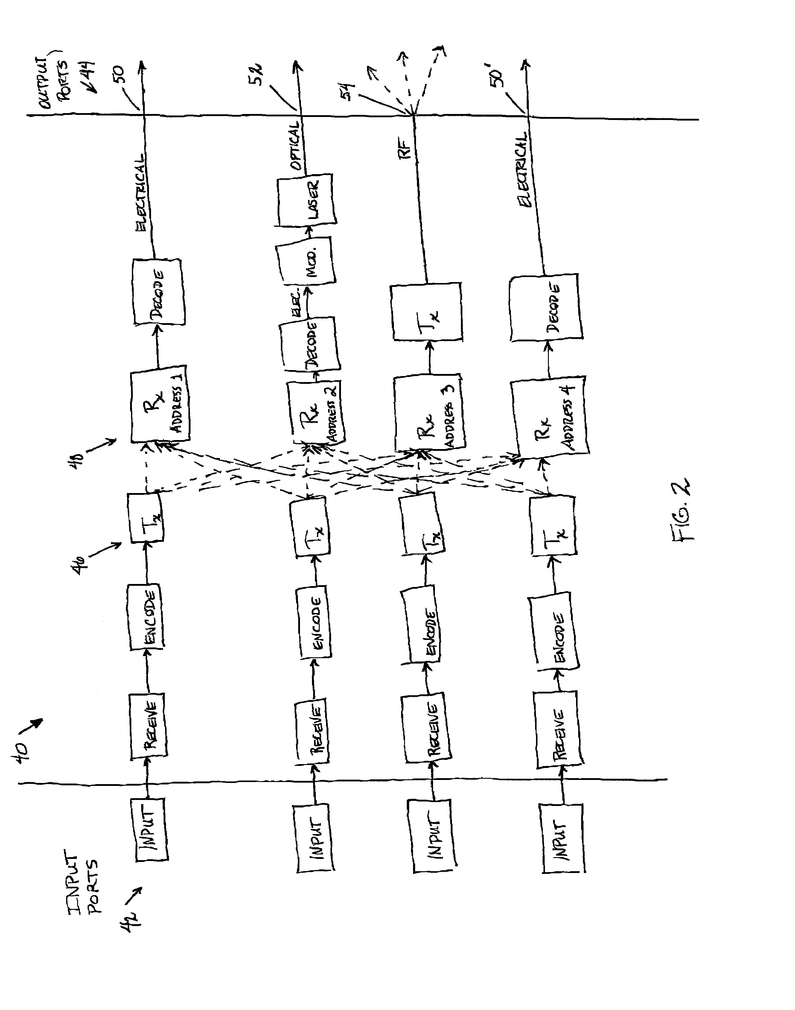
Figure 3
Abstract
Description
GOVERNMENT RIGHTS
[0001] The Government has rights to this invention pursuant to Contract No. DE-AC04-94AL85000 awarded by the U.S. Department of Energy.BACKGROUND OF THE INVENTION
[0002] 1. Field of the Invention (Technical Field)
[0003] The present invention relates to wireless communication between electronic circuit boards and between circuit components on circuit boards.
[0004] 2. Background Art
[0005] Printed circuit boards provide for the interconnection of a variety of electronic components such as integrated circuits (ICs), application specific integrated circuits (ASICs), and programmable logic devices (PLDs). Communication amongst these components is typically accomplished through etched copper traces in the circuit board. These fixed communication paths limit the flexibility of a given circuit board design, even if implemented with the latest programmable logic devices, to be reconfigured for multiple uses. Changes in the communication paths require redesign and manufacturing of a...
Examples
second embodiment
[0030]In the present invention, ATM switching and communication protocol is eliminated and interboard and intraboard communications take place directly through RF transmissions between circuit board components. Communication signals are “addressed” according to frequency and / or according to an encoding scheme to the appropriate IC I / O connection.
third embodiment
[0031]In a third embodiment, the backplane of an ATM switch is eliminated. In this embodiment, low power transmitters and receivers are used as in the first two embodiments and the switch circuit board is shielded against RF emissions to inhibit RF interference from the environment external to the switch and to inhibit the switching signals from entering the external environment. Communication data signals, such as ATM information cells, are input to and output from the circuit board through the circuit board I / O ports via any conventional means, such as fiber optics, twisted copper wire pairs, or RF transmission, but are routed via RF transmissions. This embodiment eliminates the need for a crossbar or other electronic switching matrix mechanism that is typically used in the backplane of prior art ATM switches. (Other functions of ATM switching, such as connection establishment and management, “quality of service” negotiation, and other ATM functions are still performed as required...