
Mismatch-shaping dynamic element matching systems and methods for multi-bit sigma-delta data converters
a dynamic element matching and dynamic element technology, applied in transmission systems, instruments, code conversion, etc., can solve the problems of limiting the achievable maximum input signal bandwidth, and reducing the maximum allowable input range, so as to achieve the effect of reducing the delay introduced by the dem algorithm, reducing the delay, and facilitating higher-order spectral shaping of mismatch errors
Patent Information
- Authority / Receiving Office
- US · United States
- Patent Type
- Patents(United States)
- Current Assignee / Owner
- Publication Date
- 2009-08-18
Smart Images
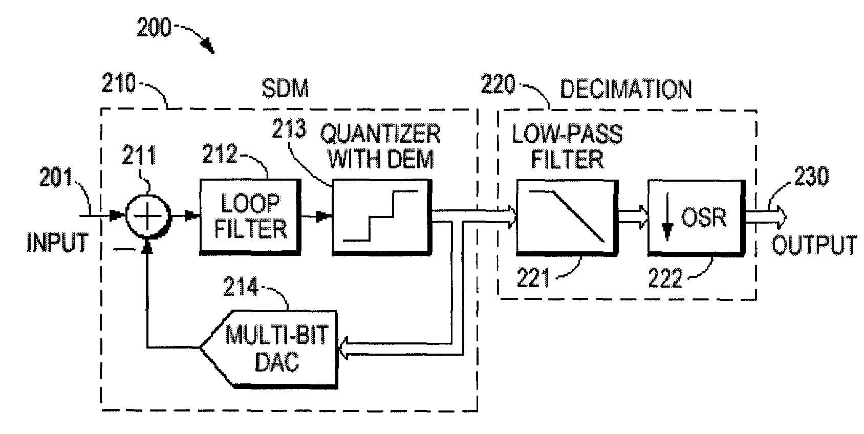
Figure 1 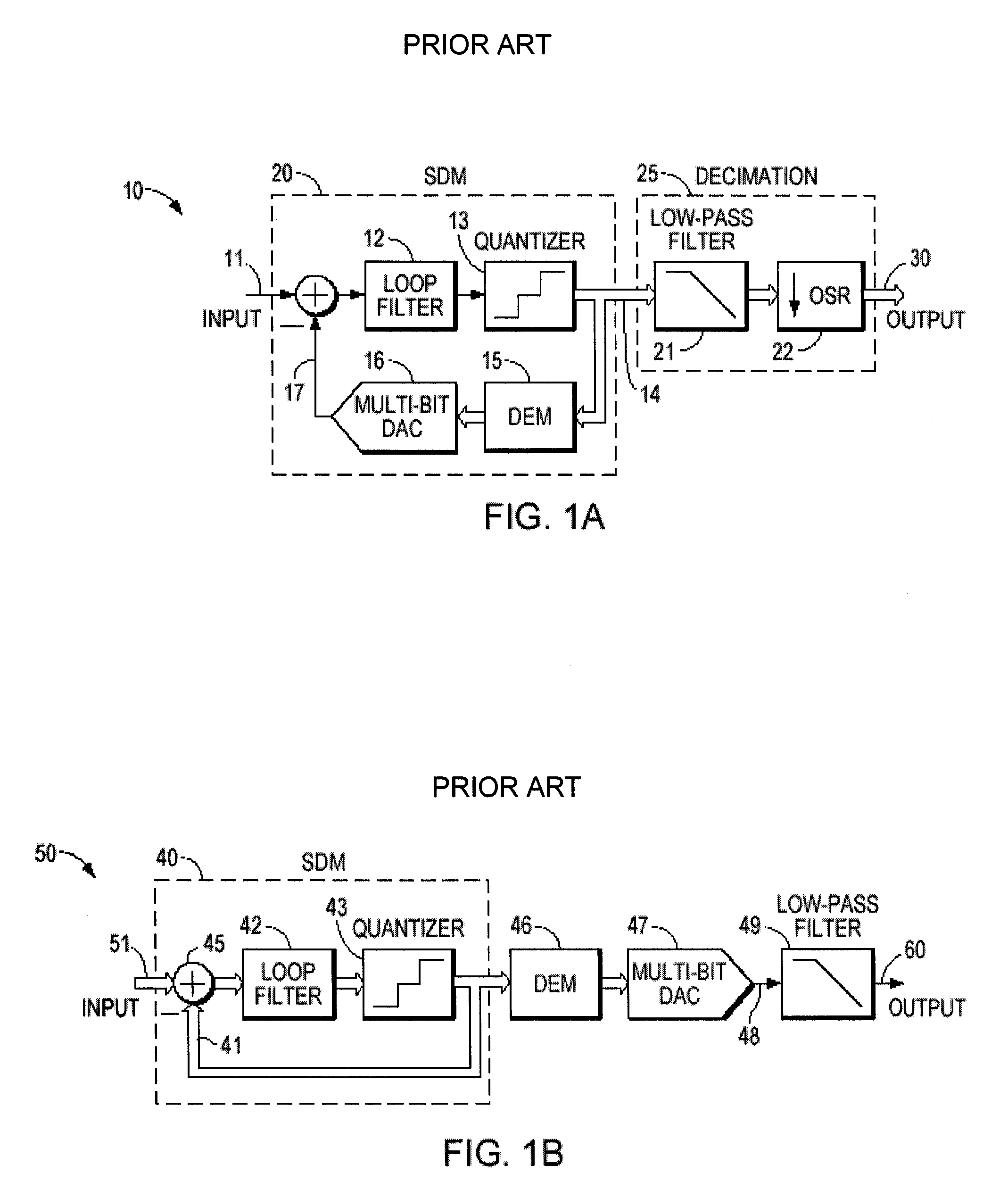
Figure 2 
Figure 3
Abstract
Description
Cross-Reference to Related Applications
[0001] This patent application claims priority to a provisional patent application serial number 60 / 792,573, filed Apr. 16, 2006, entitled “Mismatch-Shaping Dynamic Element Matching Method For Multi-Bit Sigma-Delta Data Converters,” by Mucahit Kozak, Eugene M. Petilli, and Brian Jadus. The contents of this provisional patent application are hereby incorporated by reference.
[0002] This patent application is a continuation-in-part of non-provisional patent application Ser. No. 11 / 208,430, filed Aug. 19, 2005, entitled “Hybrid Heterodyne Transmitters and Receivers,” by Eugene M. Petilli, Brian Jadus, Clyde Washburn, and John M. Alvermann. The contents of this nonprovisional patent application are hereby incorporated by reference.STATEMENT REGARDING FEDERALLY SPONSORED RESEARCH
[0003] Not applicableFIELD OF THE INVENTION
[0004] The present invention relates generally to sigma delta converters, and, in particular, to multi-bit sigma-delta data converters ...
Examples
Embodiment Construction
[0053]FIG. 1A is an illustrative block diagram of a prior art SDM ADC system, showing a top-level architecture for an SDM ADC system 10. An analog input signal 11 in an SDM 20 is subtracted from an analog feedback signal 17, and then processed by an analog feed-forward loop filter 12 before being fed into a multi-bit quantizer 13. The loop filter 12 (which can, for example, be an integrator) filters the resultant signal so as to minimize the effect of the error signal on a noise-shaping characteristic of the SDM 200. The multi-bit quantizer produces a low-resolution high-speed digital signal 14, which is converted in the feedback loop into the analog domain by a multi-bit feedback DAC 16. A digital decimation filter 25 processes the low-resolution and high-speed digital output from the multi-bit quantizer to produce a high-resolution low speed digital signal 30 at the output of the SDM ADC system.
[0054]Still referring to FIG. 1A, the analog input signal 11 to the SDM ADC system 10 h...