
Semiconductor device and electro-optical device
a technology of electrooptical devices and semiconductors, applied in the field of semiconductor devices and electrooptical devices, can solve the problems of difficult to expect constant current operation, insufficient ldd structure alone, and insufficiently suppressing the kink phenomenon. , to achieve the effect of reducing leak current, improving contrast, and uniform image display
Patent Information
- Authority / Receiving Office
- US · United States
- Patent Type
- Patents(United States)
- Current Assignee / Owner
- Publication Date
- 2009-12-01
Smart Images
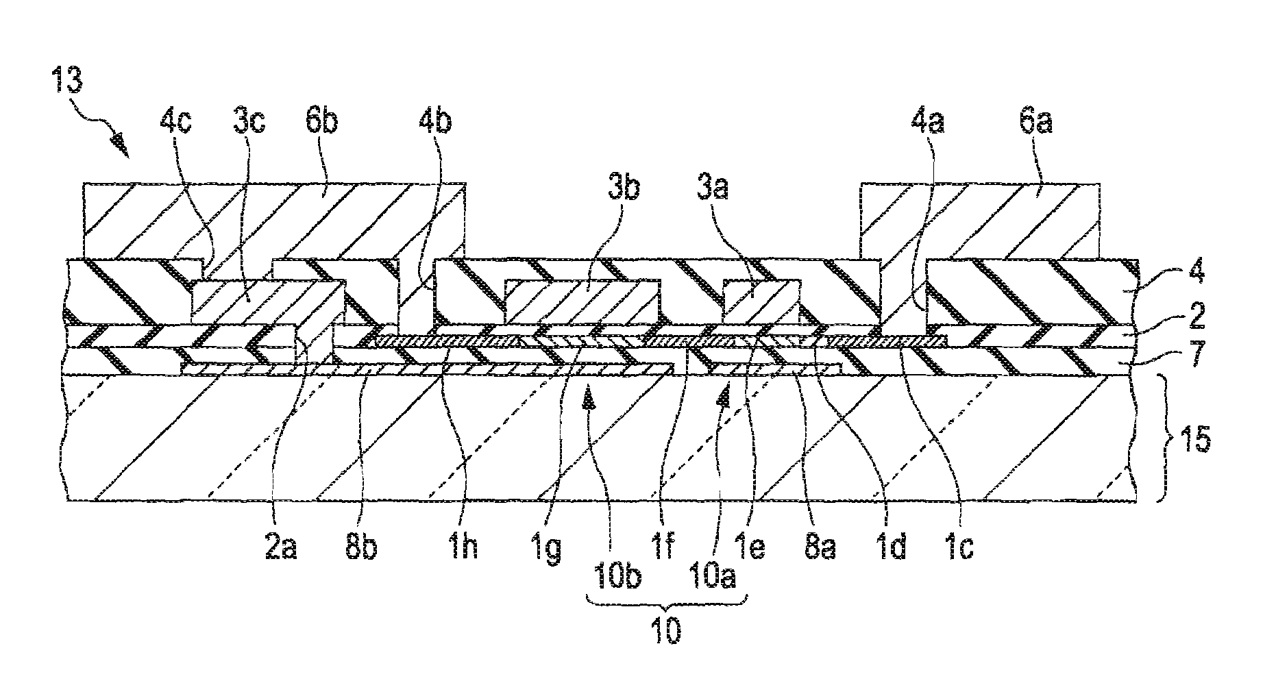
Figure 1 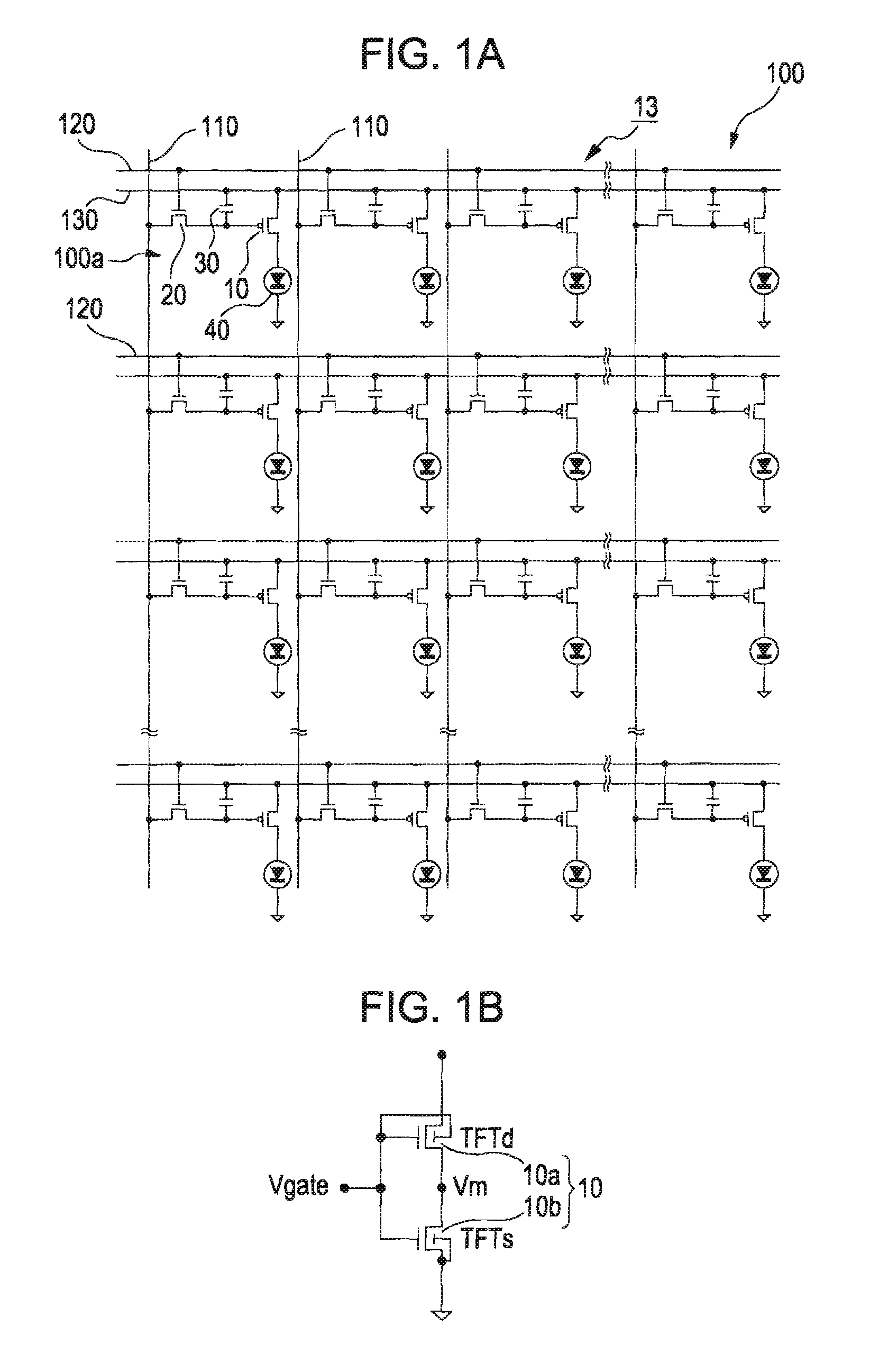
Figure 2 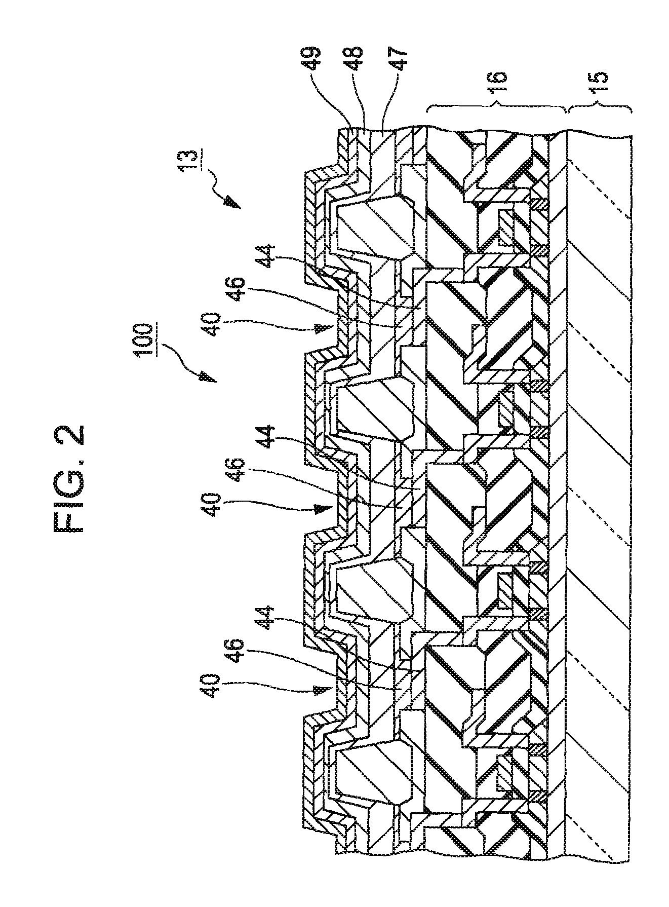
Figure 3
Abstract
Description
BACKGROUND
[0001] 1. Technical Field
[0002] The present invention relates to a semiconductor device and an electro-optical device that uses a polycrystalline silicon film disposed over a substrate as an active layer of a thin film transistor.
[0003] 2. Related Art
[0004] A thin film transistor is used as a transistor for controlling an electric current that flows into an organic electro-luminescence element of an organic electro-luminescence device. Another example of applications of a thin film transistor is a constituent element of a liquid crystal device that has analog circuits, a typical example of which is an operational amplifier, though not limited thereto, formed on the same single built-in circuit board thereof. In these non-limiting exemplary applications of a thin film transistor, the saturation characteristics of the thin film transistor are utilized in comparison with the counterpart of a MOS transistor that is formed on a silicon substrate, it is known that the saturation cha...
Examples
embodiment 1
General Configuration of Light-emitting Device
[0042]FIG. 1A is a general circuit diagram that schematically illustrates an example of the electric configuration of an organic EL device to which the invention is applied, whereas FIG. 1B is an equivalent circuit diagram of a thin film transistor for electric current control to which the invention is applied. A light-emitting device (apparatus) 100 that is illustrated in FIG. 1 is configured to drive an organic EL element 40, which emits light when a driving current flows through the organic EL element 40, by means of a thin film transistor. Such a type of light-emitting device does not require any backlight because the organic EL element 40 emits light in a self-luminous manner. As another example of advantages thereof, it offers less angle-dependent visibility.
[0043]The light-emitting device 100 has a plurality of scanning lines 120, a plurality of data lines 110 that extend in a direction orthogonal to the extending direction of the...
improvement example of embodiment 1
[0081]In the exemplary embodiment of the invention described above, the drain-side back gate electrode 8a is formed at a region that overlaps the whole length of the first channel region 1e. In addition, the source-side back gate electrode 8b is formed at a region that overlaps the whole length of the second channel region 1g. However, as illustrated in FIGS. 9A and 9B, it is preferable that the source-side back gate electrode 8b should be formed at a region that overlaps not the whole length but the partial length of the second channel region 1g; more specifically, it is preferable that the source-side back gate electrode 8b should be formed at a region that overlaps the source end of the second channel region 1g but not the drain end thereof in such a manner the drain end of the source-side back gate electrode 8b lies under a “halfway point” that falls short of, that is, does not reach, the drain end of the second channel region 1g when viewed in a direction going from the source ...
example of embodiment 1
Variation Example of Embodiment 1
[0083]In the first exemplary embodiment of the invention described above, both of the drain-side back gate electrode 8a and the source-side back gate electrode 8b are formed. As a variation example of the configuration described above, the source-side back gate electrode 8b only may be formed.