
Semiconductor device
a technology of semiconductors and devices, applied in the field of semiconductor devices, can solve the problems of complicated control and significant impact on the chip area, and achieve the effects of reducing the offset time until the start of the chip operation, increasing the number of conforming products, and reducing the time required to transfer relief information after power is turned on
Patent Information
- Authority / Receiving Office
- US · United States
- Patent Type
- Patents(United States)
- Current Assignee / Owner
- Publication Date
- 2010-08-24
Smart Images
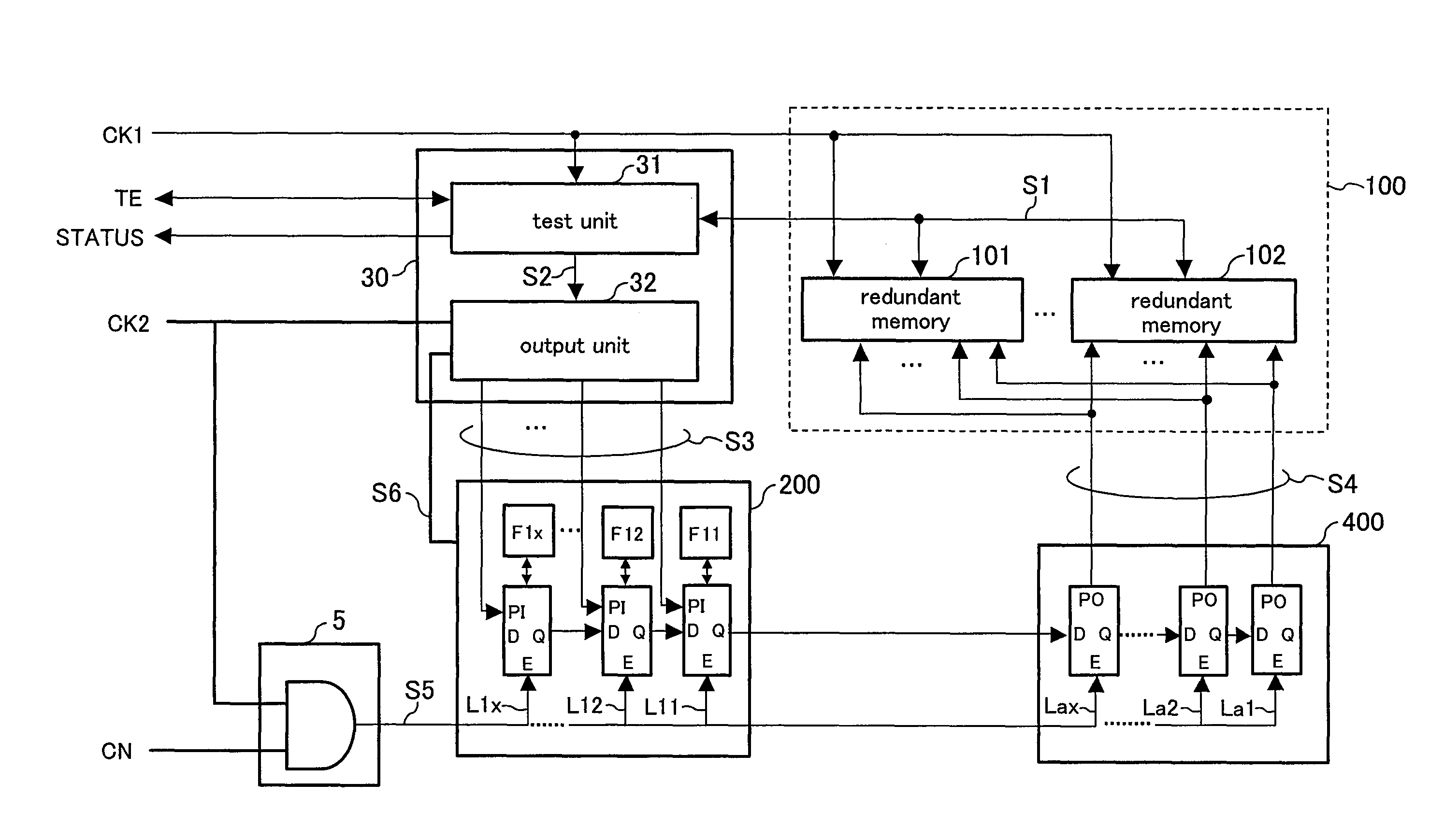
Figure 1 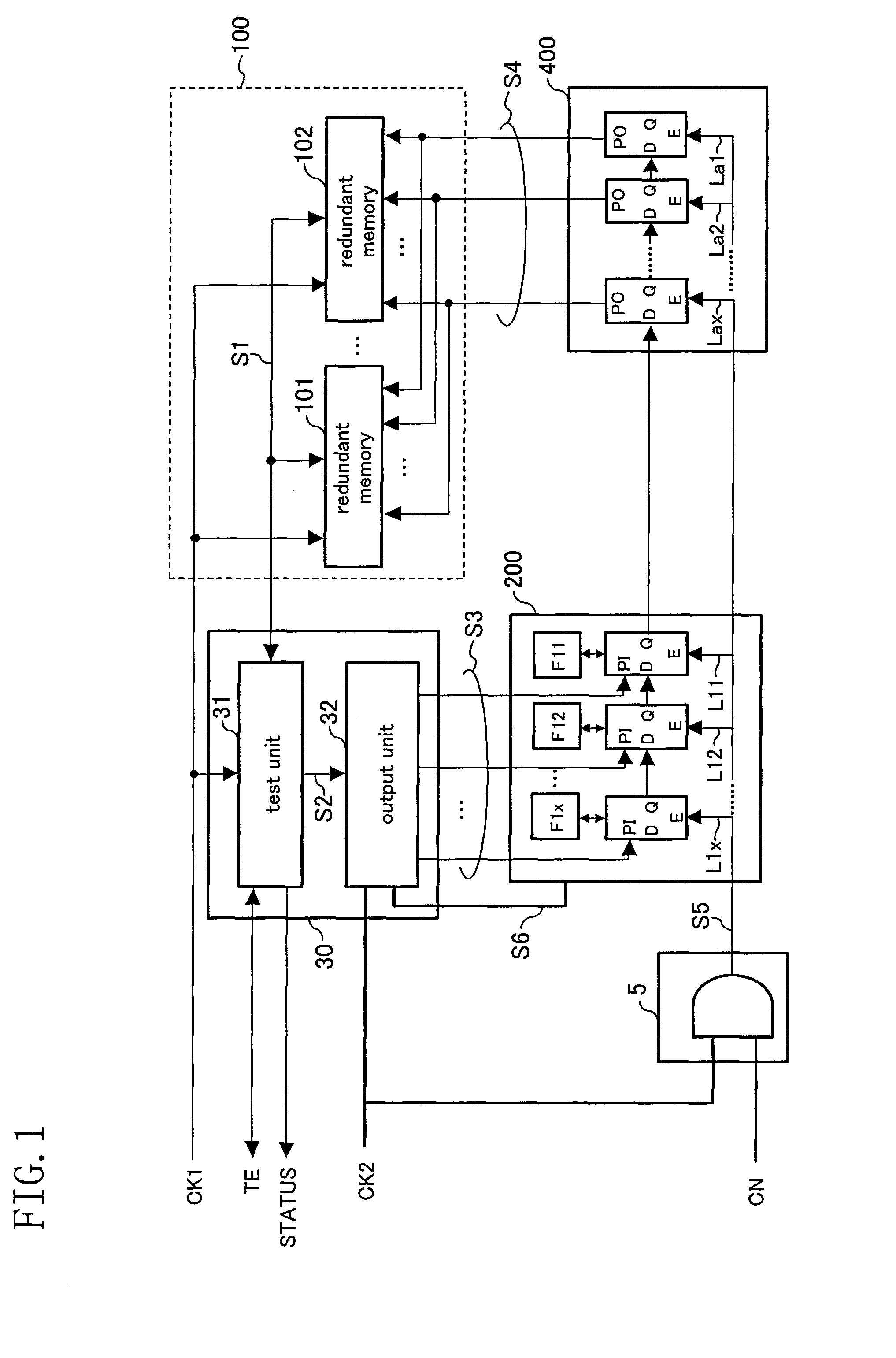
Figure 2 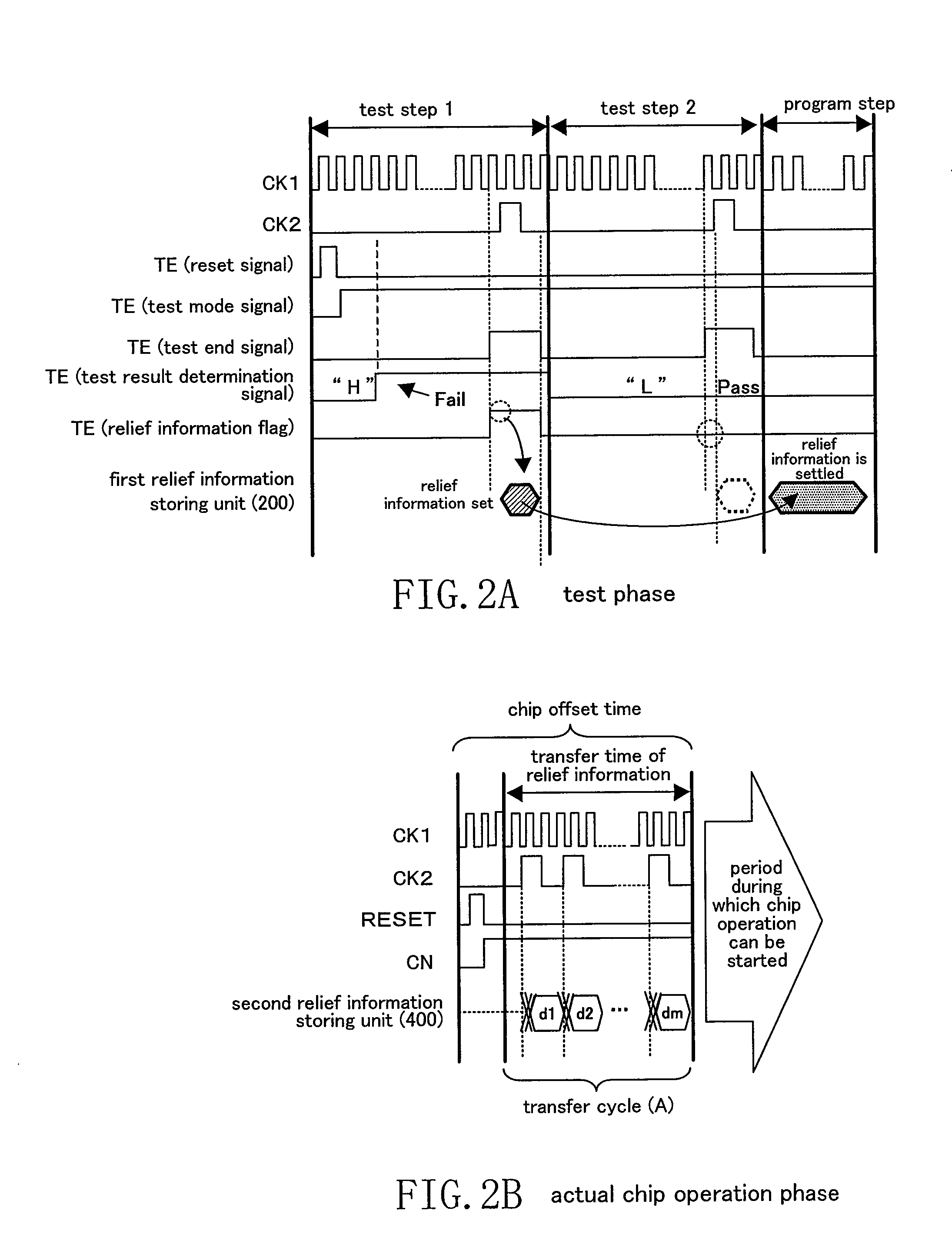
Figure 3
Abstract
Description
CROSS REFERENCE TO RELATED APPLICATIONS
[0001] This Non-provisional application claims priority under 35 U.S.C. §119(a) on Patent Application No. 2007-268870 filed in Japan on Oct. 16, 2007, the entire contents of which are hereby incorporated by reference.BACKGROUND OF THE INVENTION
[0002] 1. Field of the Invention
[0003] The present invention relates to a semiconductor device having a so-called redundant memory.
[0004] 2. Description of the Related Art
[0005] Conventionally, a method for efficiently transferring relief information (repairing / replacement information) to a memory with a redundancy scheme (hereinafter simply referred to as a “redundant memory”) in which a defect occurring in a memory array can be relieved (repaired / replaced), has been proposed (see, for example, Patent Document 1).
[0006] Patent Document 1: U.S. Pat. No. 6,556,490SUMMARY OF THE INVENTION
[0007] As the scale of a system LSI increases, the total capacity or the number of memories mounted on a chip increases. Also, t...
Examples
first embodiment
[0029]FIG. 1 is a block diagram showing a configuration of a semiconductor device according to a first embodiment of the present invention. FIGS. 2A and 2B are timing charts showing an operation relating to repairing / replacement by a redundancy scheme of the semiconductor device of this embodiment. FIG. 2A shows a test phase and FIG. 2B shows an actual chip operation phase.
[0030]In FIG. 1, the semiconductor device comprises redundant memories 101 and 102 having a plurality of memory cells and having a function of relieving (repairing / replacing) a defective memory cell (defective cell), a first relief information storing unit 200 for storing relief information (repairing / replacement information) for relieving (repairing / replacing) the redundant memories 101 and 102 having a defective cell, and a second relief information storing unit 400 for receiving and storing relief information transferred from the first relief information storing unit 200. The second relief information storing u...
second embodiment
[0044]FIG. 3 is a block diagram showing a configuration of a semiconductor device according to a second embodiment of the present invention. FIG. 4 is a timing chart showing an operation of transferring relief information, of operations relating to repairing / replacement by a redundancy scheme in the semiconductor device of this embodiment.
[0045]The configuration of FIG. 3 is basically similar to that of FIG. 1. In FIG. 3, there are a plurality of combinations (five in FIG. 3) each of which includes a second relief information storing unit and a plurality of redundant memories sharing the unit. Specifically, the semiconductor device of FIG. 3 comprises second relief information storing units 400-1 to 400-5, a sharing redundant memory group 100 including redundant memories 101 and 102, and a sharing redundant memory group 110 including redundant memories 111, 112 and 113. The second relief information storing unit 400-1 is shared by the redundant memories 101 and 102, and the second r...