
Methods to generate state space models by closed forms for general interconnect and transmission lines, trees and nets, and their model reduction and simulations
a technology of state space and closed forms, applied in the direction of instrumentation, program control, cad circuit design, etc., can solve the problems of vlsi circuit design performance, interconnect delay dominating gate delay, and inability to accurately capture the original model
Patent Information
- Authority / Receiving Office
- US · United States
- Patent Type
- Patents(United States)
- Current Assignee / Owner
- Publication Date
- 2010-09-28
Smart Images
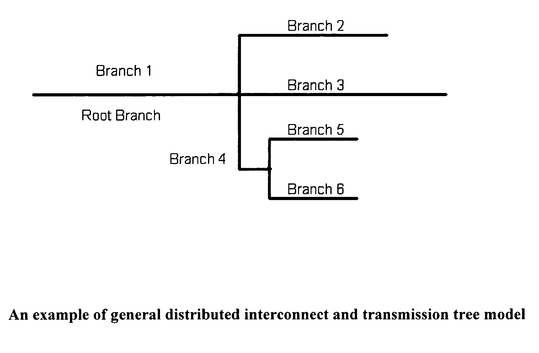
Figure 1 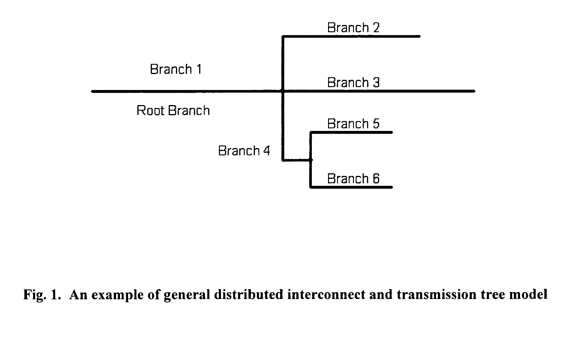
Figure 2 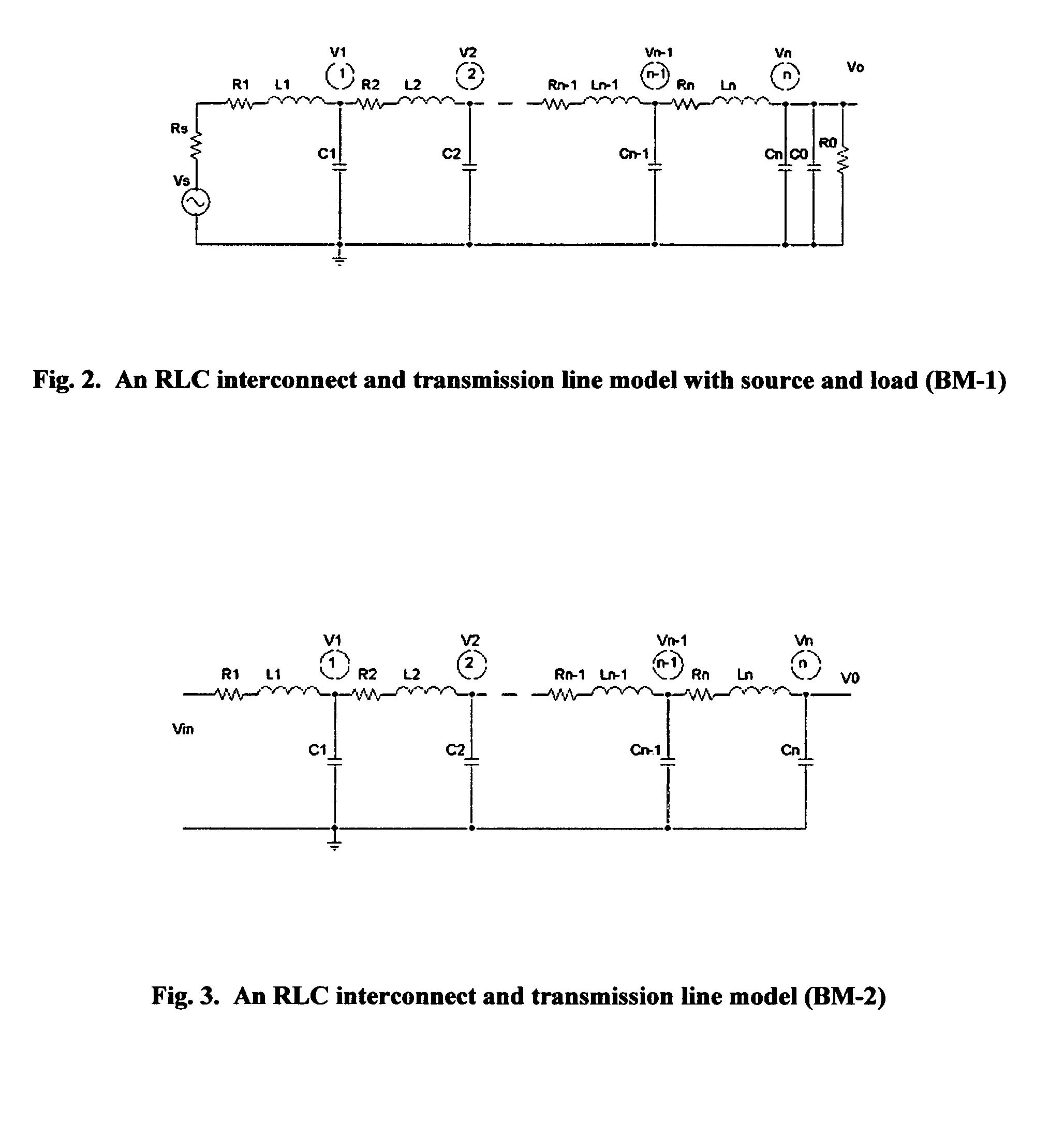
Figure 3
Abstract
Description
CROSS-REFERENCE TO RELATED APPLICATIONS
[0001] Not ApplicableSTATEMENT REGARDING FEDERALLY SPONSORED RESEARCH OR DEVELOPMENT
[0002] Not ApplicableREFERENCE TO SEQUENCE LISTING, A TABLE, OR A COMPUTER PROGRAM LISTING COMPACT DISK APPENDIX
[0003] Not ApplicableBACKGROUND OF THE INVENTION
[0004] 1. Field of the Invention
[0005] The present invention relates to general interconnect and transmission lines, trees and nets, and methods to obtain their state space models in time domain, and their simulations for their characteristics and evolution, and their practice for various model reduction methods, and optimization methods.
[0006] 2. Description of the Related Art
[0007] With the rapid increase of integration level and speed, IC interconnect has become one of important limiting factors of today's VLSI circuit design performance. It has been commonly recognized that interconnect delay dominates gate delay in current deep submicron VLSI circuits. The average length of the chip interconnect and the chi...
Examples
case 1
[0175] Consider an evenly distributed RLC interconnect BM-3 of 0.01 cm long with distribution characteristic data of resistor 5.5 kΩ / m and capacitor 94.2 pF / m. An 200th-order model is used as its original model with R=5.5·10−3Ω and C=9.42·10−5 pF, while the inductor value L is calculated from the light speed in the material and the capacitor value C. It leads to L=2.831×10⁻¹³ H. Also, to show some feature of RLC interconnect, this distributed interconnect line has a source resistor Rs=200Ω and a load resistor R0=1MΩ, i.e., a kind of BM-3.
case 2
[0176] Consider a distributed RLC interconnect tree with 6 evenly distributed interconnect branch lines connected as FIG. 1, as an example of a general ITLTAN to show the new methods described above. The branch lengths are as follows: l1=l2=l3=0.01 cm and l4=l5=l6=0.005 cm. Their distribution characteristic data are the same as Case 1, i.e., of resistor 5.5 kΩ / m, capacitor 94.2 pF / m and L=2.831×10⁻⁷H / m. Take a branch order of 200 for each branch of branch 1-3, and 100 for each branch of branches 4-6. Thus, branches 1-3 have their parameters Re1=5.5·10−3Ω, Ce1=9.42·10−5 pF and Le1=0.2831 pH, with order 200, i.e., N1b=N2b=N3b=200, and n1b=n2b=n3b=100. Branches 4-6 have the same parameters as Re2=5.5·10−3Ω, Ce2=9.42·10−5 pF and Le2=0.2831 pH, but with order 100, i.e., N4b=N5b=N6b=100 and n4b=n5b=n6b=50. Branch 1 has a source resistor Rs=200Ω. Branches 2, 3, 5 and 6 have their respective load R01 MΩ and load capacitors C0=0.1 F. Select the terminal voltage of branch 6 as an output for a...