

Chip testing circuit
a testing circuit and data compression technology, applied in testing circuits, individual semiconductor device testing, instruments, etc., can solve the problems of increasing the number of pins for testing, increasing the cost of the chip testing circuit, increasing the whole production cost, etc., to increase the testing efficiency, reduce production costs, increase testing throughput per unit time
Patent Information
- Authority / Receiving Office
- US · United States
- Patent Type
- Patents(United States)
- Current Assignee / Owner
- Publication Date
- 2012-05-01
Smart Images
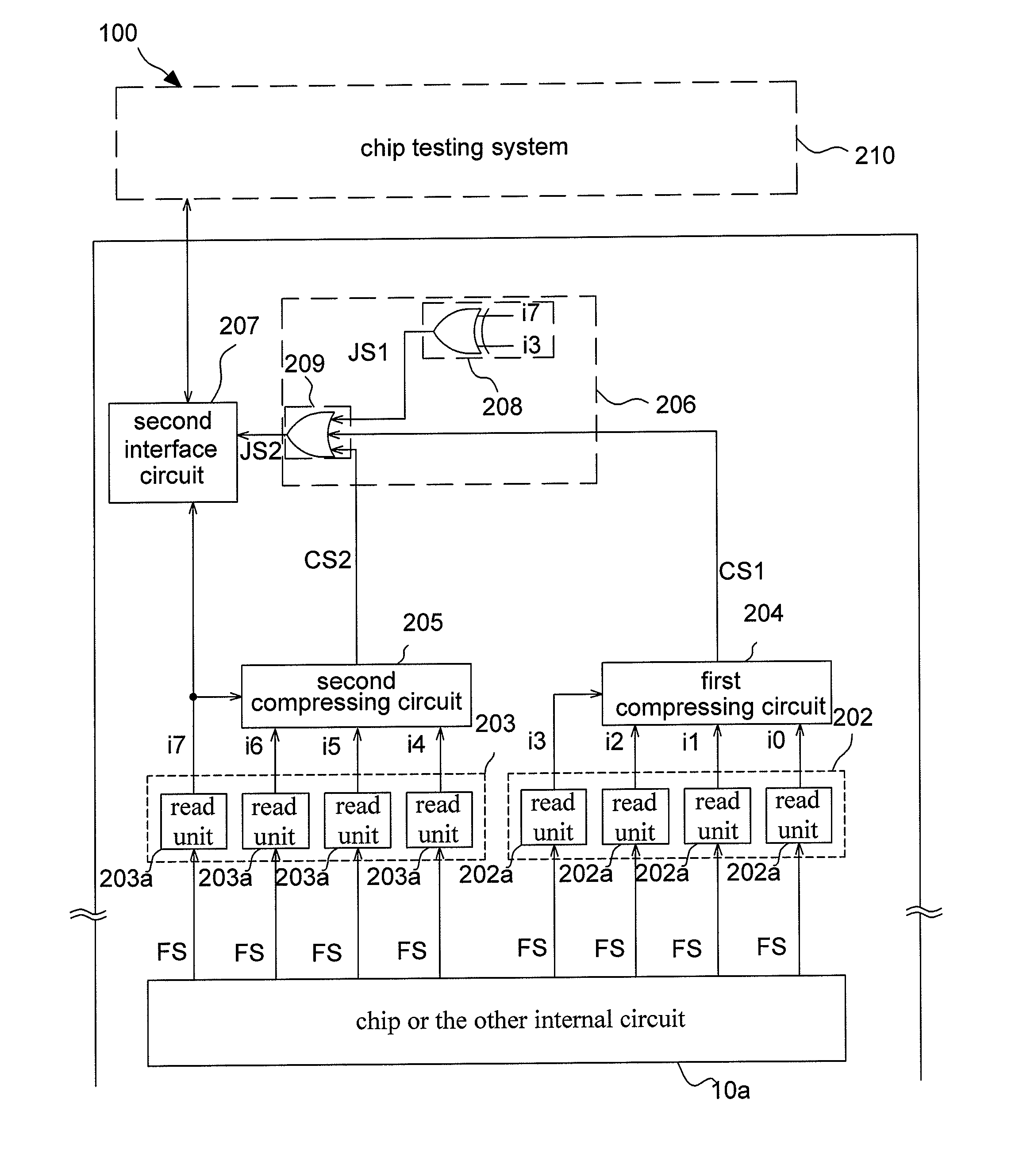
Figure 1 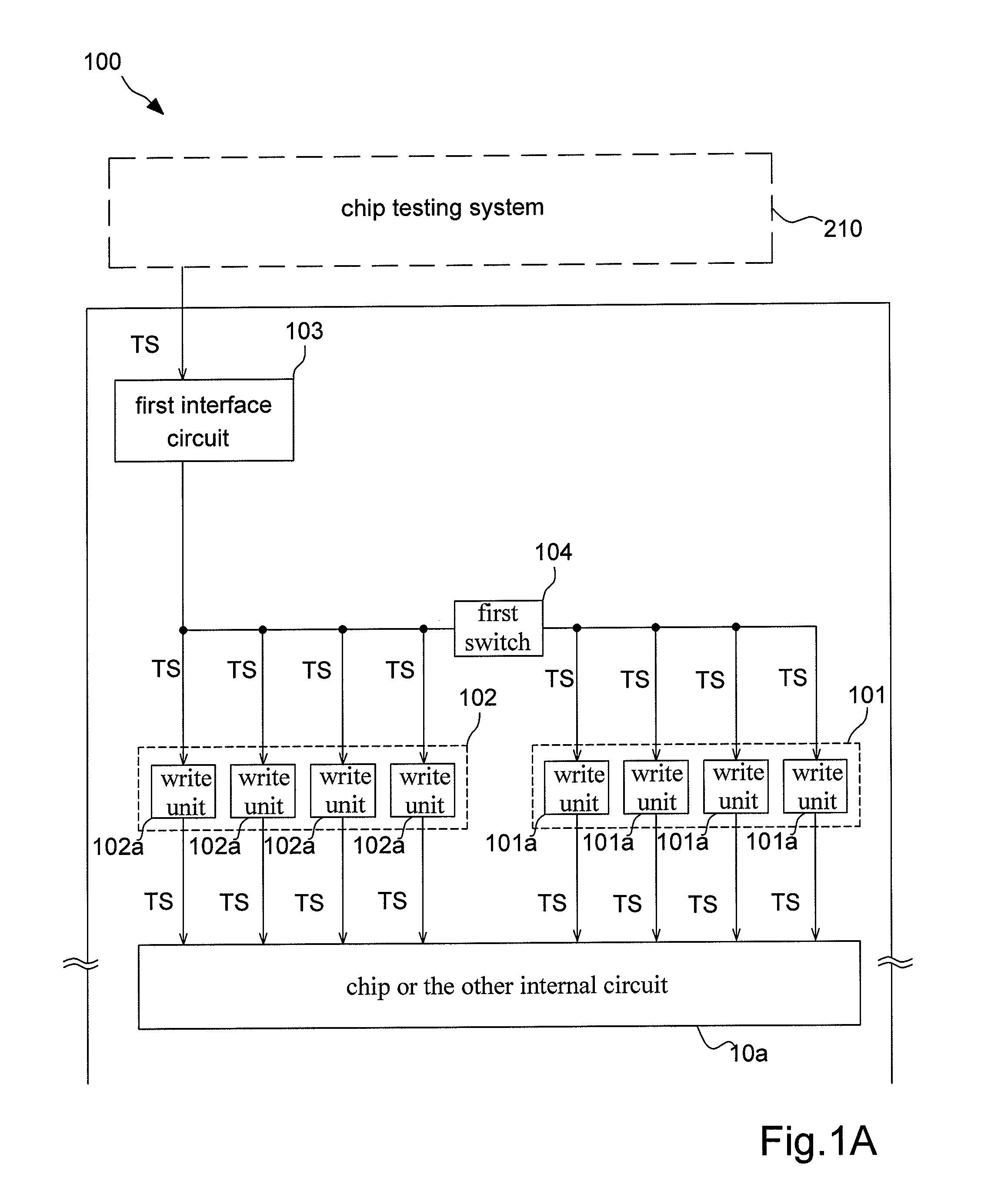
Figure 2 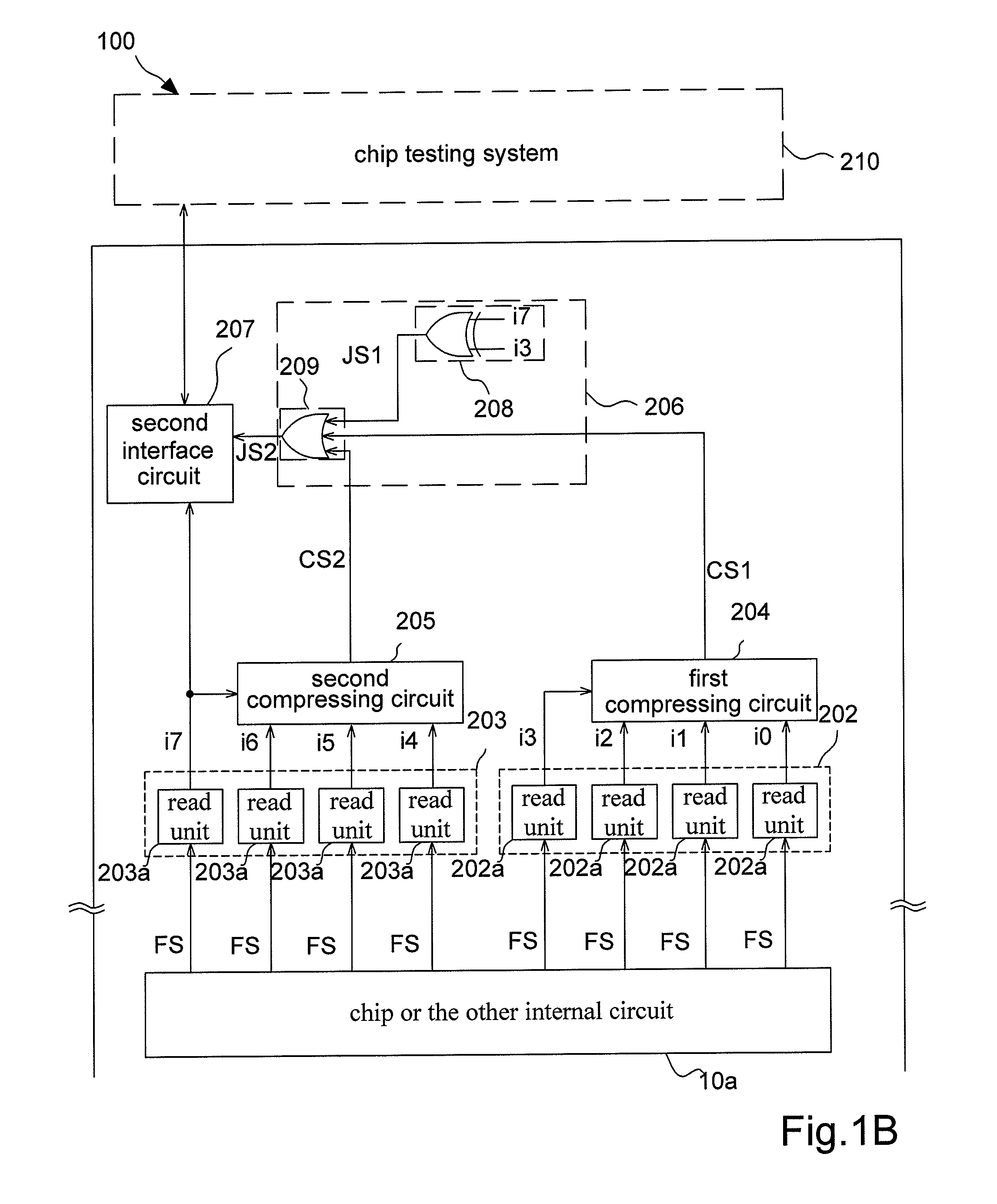
Figure 3
Abstract
Description
BACKGROUND OF THE INVENTION
[0001] (a) Field of the Invention
[0002] The invention relates to a chip data compressing test multiplexing circuit, particularly to a chip data compressing test multiplexing circuit for increasing testing throughput.
[0003] (b) Description of the Related Art
[0004] An integrate circuit (IC) is one of essential electronic elements for an information appliance because of its great functionality and compact size. In order to assure the functionality of a chip, the chip is required to pass comprehensive tests. Generally, the test method is to input a known testing signal into the circuit in the chip and acquire a feedback signal from the circuit of the chip to thereby determine whether the chip functions normally or not.
[0005] However, in order to correctly test a chip, the architecture of the chip testing circuit according to the prior art, for example one cycle IO compress 8 read circuit to test 8 signals at once, should have two pins only for testing and two inter...
Examples
Embodiment Construction
[0013]FIG. 1A and FIG. 1B show schematic diagrams illustrating the chip testing circuit (chip data compressing test multiplexing circuit) according to one embodiment of the invention. The chip testing circuit 100 according to one embodiment of the invention comprises a write circuit portion to input the testing signal TS to the chip or the other internal circuit 10a, as shown in FIG. 1A and a read circuit portion to receive the feedback signal FS from the chip or the other internal circuit 10a, as shown in FIG. 1B.
[0014]As shown in FIG. 1A, the write circuit of the chip testing circuit 100 according to one embodiment of the invention comprises a first write compressing circuit 101, a second write compressing circuit 102, a first interface circuit 103, and a first switch 104.
[0015]In this embodiment, the first write compressing circuit 101 and the second write compressing circuit 102 separately comprise four write units, that is, the first group of write units 101a and the second gro...