
Structure and method for self protection of power device with expanded voltage ranges
a power device and voltage range technology, applied in the direction of semiconductor devices, semiconductor/solid-state device details, electrical apparatus, etc., can solve the problems of unfavorable manufacturing and operation costs, increase in die size, and damage to other components
Patent Information
- Authority / Receiving Office
- US · United States
- Patent Type
- Patents(United States)
- Current Assignee / Owner
- Publication Date
- 2013-05-14
- Estimated Expiration
- Not applicable · inactive patent
Smart Images
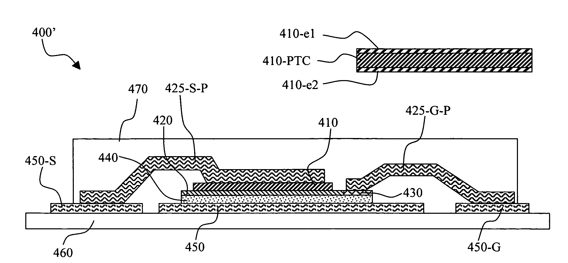
Figure 1 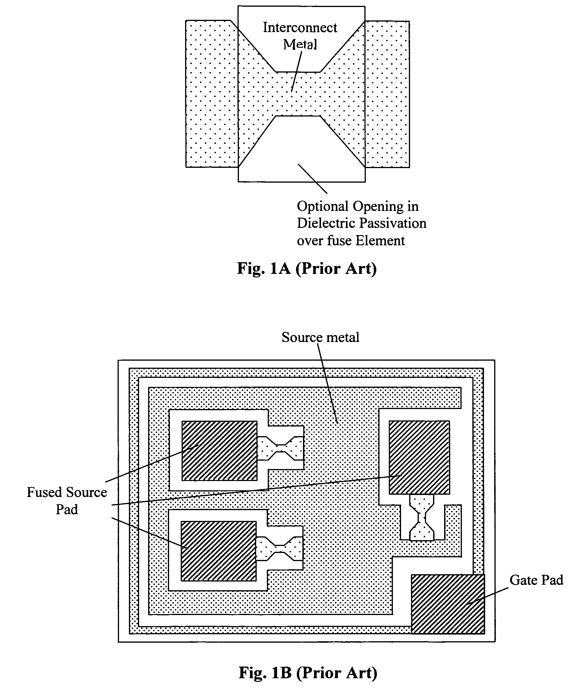
Figure 2 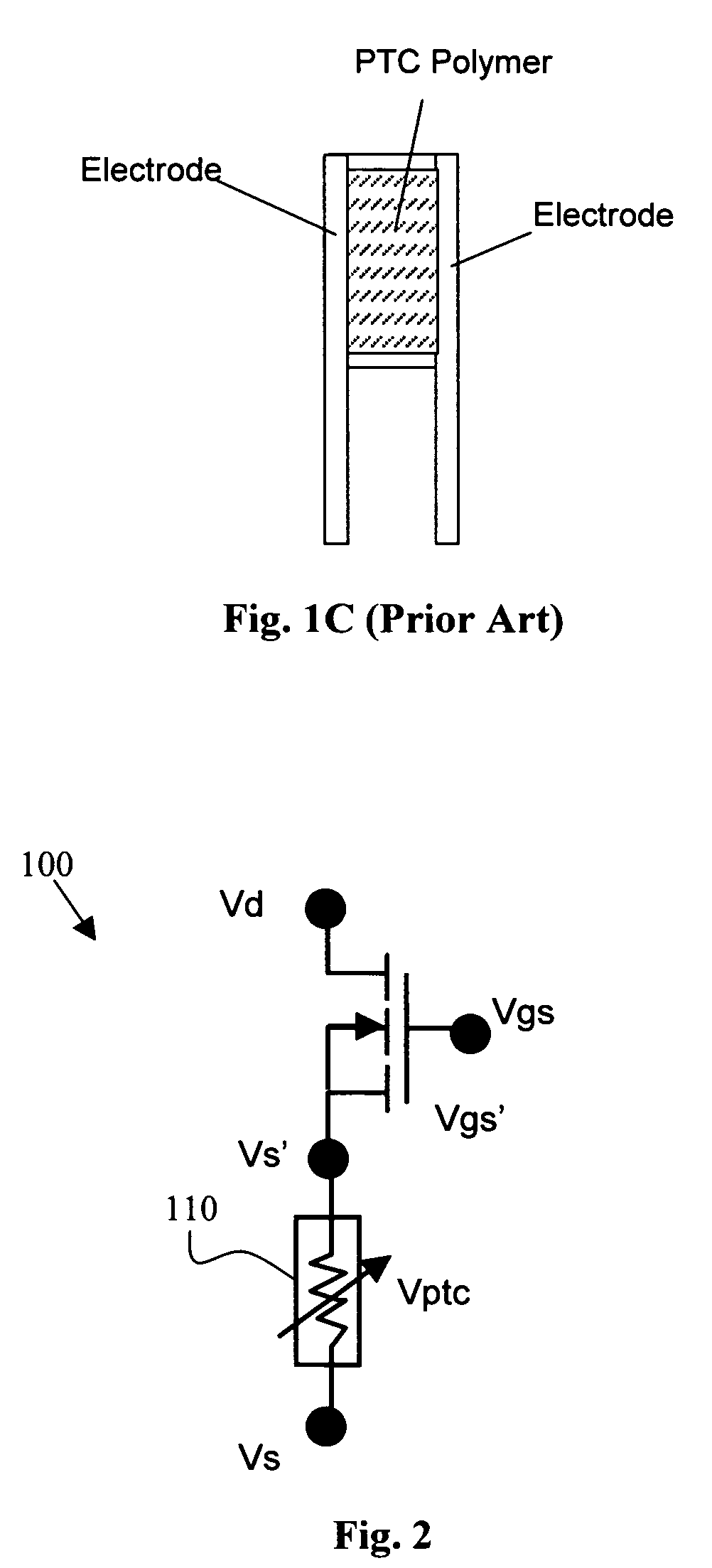
Figure 3
Abstract
Description
[0001] This application is a Continuation in Part (CIP) Application and claims priority to pending U.S. patent application entitled “STRUCTURE AND METHOD FOR SELF PROTECTION OF POWER DEVICE” filed on Jan. 25, 2007 and accorded Ser. No. 11 / 657,862 by a common Applicant of this Application, the benefit of its filing date being hereby claimed under Title 35 of the United States Code.BACKGROUND OF THE INVENTION
[0002] 1. Field of the Invention
[0003] The invention relates generally to a device configuration and method of protecting the device. More particularly, this invention relates to an improved circuit configuration and method of protecting active devices operated at a high voltage from damages due to over current caused by an electrical short by using a conductive material with a positive temperature coefficient.
[0004] 2. Description of the Relevant Art
[0005] Under high power conditions, the power devices often fail in a “short circuit” condition and that can result in damages to other c...
Examples
Embodiment Construction
[0029]FIG. 2 is a schematic representation of a PTC protected FET 100, (which can also be referred to as a fuse FET) that includes a resistor 110 composed of a material that has a positive temperature coefficient (PTC) and configured as a conductive layer connected to a source electrode and further provides a feedback voltage to regulate the gate-source voltage. As the temperature of the device under protection is increased, the resistance of the PTC resistor 110 is also increased and the resistance is drastically increased once the PTC trip temperature is reached. In this protection configuration, any source to drain current (Ids) increase will result in a voltage drop Vptc across the PTC structure 110 thus reducing the FET control voltage Vgs. Specifically, the voltages have functional relationships that can be represented as:
Vgs=Vgs′+Vptc
Vgs′=Vgs−Vptc
[0030]When the temperature of the device is above the trip temperature of the PTC, the voltage drop across the PTC structure Vptc...