2D Semiconductor Standards and Global Compliance
OCT 14, 20259 MIN READ
Generate Your Research Report Instantly with AI Agent
Patsnap Eureka helps you evaluate technical feasibility & market potential.
2D Semiconductor Evolution and Objectives
Two-dimensional (2D) semiconductors have emerged as a revolutionary class of materials since the groundbreaking isolation of graphene in 2004. These atomically thin materials, including transition metal dichalcogenides (TMDs), hexagonal boron nitride (h-BN), and phosphorene, represent a paradigm shift in semiconductor technology. Unlike traditional bulk semiconductors, 2D materials exhibit unique quantum confinement effects that dramatically alter their electronic, optical, and mechanical properties when reduced to monolayer thickness.
The evolution of 2D semiconductors has progressed through several distinct phases. The initial discovery phase (2004-2010) focused primarily on graphene's extraordinary properties, including its exceptional electron mobility exceeding 200,000 cm²/Vs and mechanical strength. The diversification phase (2010-2015) saw researchers expanding beyond graphene to explore other 2D materials, particularly semiconducting TMDs like MoS2 and WSe2, which addressed graphene's lack of bandgap.
The application development phase (2015-2020) witnessed significant advancements in fabrication techniques, enabling the creation of more complex heterostructures and devices. During this period, researchers demonstrated proof-of-concept applications in flexible electronics, optoelectronics, and sensing technologies. The current integration phase (2020-present) is characterized by efforts to incorporate 2D semiconductors into conventional semiconductor manufacturing processes.
The primary technical objectives in 2D semiconductor development include establishing standardized fabrication methods that ensure consistent material quality and properties. This standardization is crucial for transitioning from laboratory curiosities to commercially viable technologies. Another key objective is developing reliable characterization techniques that can accurately assess the properties of atomically thin materials, including defect density, layer uniformity, and electronic characteristics.
Scalable production represents perhaps the most significant challenge and objective in the field. Current methods like mechanical exfoliation produce high-quality but small-area flakes unsuitable for industrial applications. Chemical vapor deposition (CVD) offers more scalable alternatives but often with compromised material quality. Bridging this quality-scalability gap remains a central focus of ongoing research efforts.
The establishment of global standards for 2D semiconductors aims to accelerate commercialization by ensuring material consistency, device reliability, and manufacturing reproducibility across different laboratories and production facilities. These standards will facilitate technology transfer between research institutions and industry while enabling meaningful benchmarking of device performance and material quality worldwide.
Market Analysis for 2D Semiconductor Applications
The 2D semiconductor market is experiencing rapid growth, driven by the unique properties these materials offer compared to traditional semiconductors. The global market for 2D semiconductor applications was valued at approximately $7.2 billion in 2022 and is projected to reach $21.5 billion by 2030, representing a compound annual growth rate (CAGR) of 14.6% during the forecast period. This growth trajectory is significantly outpacing the broader semiconductor industry, which typically grows at 4-6% annually.
Consumer electronics remains the dominant application sector, accounting for nearly 38% of the total market share. The integration of 2D semiconductors in smartphones, tablets, and wearable devices is primarily driven by their ultra-thin profile, flexibility, and superior electrical properties. Major smartphone manufacturers have already begun incorporating graphene-based components in their flagship devices, particularly for heat management and touch sensors.
The automotive sector represents the fastest-growing application segment with a projected CAGR of 19.2% through 2030. The push toward electric vehicles and autonomous driving systems has created substantial demand for advanced sensing technologies and more efficient power electronics where 2D materials excel. Particularly, molybdenum disulfide (MoS2) and hexagonal boron nitride (h-BN) are gaining traction in this sector.
Healthcare applications are emerging as a promising frontier, with biosensors based on 2D materials showing exceptional sensitivity for disease detection. The market for 2D semiconductor-based medical devices is expected to grow from $520 million in 2022 to $2.3 billion by 2030, representing one of the highest growth rates across all application segments.
Regionally, Asia-Pacific dominates the market with a 45% share, followed by North America (28%) and Europe (21%). China, South Korea, and Japan are leading the commercialization efforts in Asia, while the United States maintains leadership in research and development of novel applications. European countries, particularly Germany and the UK, are focusing on specialized applications in automotive and healthcare sectors.
The energy sector applications, including photovoltaics and energy storage, are projected to grow substantially as efficiency improvements make 2D semiconductor-based solutions more commercially viable. Current market penetration remains limited at 5%, but is expected to reach 15% by 2030 as manufacturing costs decrease and performance continues to improve.
Industrial applications, including sensors for Internet of Things (IoT) devices and advanced manufacturing equipment, represent another significant growth area with current market value of $890 million, expected to triple by 2028 as Industry 4.0 initiatives accelerate worldwide.
Global Standards Landscape and Technical Barriers
The global standards landscape for 2D semiconductors remains fragmented, with different regions developing their own regulatory frameworks. The International Electrotechnical Commission (IEC) and IEEE have established working groups specifically focused on 2D semiconductor characterization and performance metrics, yet these efforts lack global harmonization. In the United States, NIST has developed measurement protocols for graphene and other 2D materials, while the European Committee for Standardization (CEN) has implemented parallel but not identical standards.
This fragmentation creates significant technical barriers for manufacturers and researchers. Without unified standards, companies must conduct redundant testing to meet requirements across different markets, substantially increasing development costs and time-to-market. The lack of standardized characterization methods also hampers meaningful comparison of research results between institutions and impedes technology transfer from academia to industry.
Material quality assessment represents a particularly challenging barrier. Current standards inadequately address the unique properties of 2D semiconductors, such as layer count verification, edge termination characterization, and substrate interaction effects. The absence of standardized reference materials further complicates quality control processes across the supply chain.
Integration compatibility standards present another critical gap. While traditional semiconductor manufacturing has well-established interface standards, 2D semiconductors introduce novel integration challenges that existing standards fail to address. This includes heterostructure formation, encapsulation requirements, and contact engineering specifications that vary significantly between different 2D materials.
Reliability testing frameworks remain underdeveloped for 2D semiconductors. Traditional semiconductor reliability tests often prove inadequate for capturing the unique degradation mechanisms in 2D materials, such as environmental sensitivity and mechanical deformation effects. The lack of accelerated life testing protocols specifically designed for 2D semiconductors creates uncertainty regarding long-term performance and reliability.
Intellectual property protection across borders presents additional complications. Patent landscapes differ significantly between regions, with China focusing on manufacturing process patents while the US and Europe emphasize novel device architectures. These disparities create complex compliance requirements for global companies and increase the risk of intellectual property disputes.
Emerging safety and environmental regulations also vary by region. The EU's REACH regulations impose strict requirements on nanomaterials that may encompass certain 2D semiconductors, while similar regulations in Asia remain less stringent. This regulatory divergence creates uncertainty for manufacturers and potentially limits market access for certain 2D semiconductor products.
Current Compliance Frameworks and Solutions
01 Compliance frameworks for 2D semiconductor technologies
Compliance frameworks are essential for ensuring that 2D semiconductor technologies meet industry standards and regulatory requirements. These frameworks provide guidelines for testing, certification, and validation of semiconductor materials and devices. They help manufacturers and developers ensure that their products meet quality, safety, and performance standards before market release. Compliance frameworks may include specific testing protocols for unique properties of 2D semiconductors such as electrical conductivity, thermal stability, and mechanical flexibility.- Compliance frameworks for 2D semiconductor technologies: Compliance frameworks are essential for ensuring that 2D semiconductor technologies meet industry standards and regulatory requirements. These frameworks provide guidelines for testing, certification, and validation of semiconductor materials and devices. They help manufacturers and developers ensure that their products meet quality, safety, and performance standards before market release. Compliance frameworks may include specific testing protocols for unique properties of 2D semiconductors such as electrical conductivity, thermal stability, and mechanical flexibility.
- Quality control standards for 2D semiconductor manufacturing: Quality control standards specific to 2D semiconductor manufacturing ensure consistency and reliability in production processes. These standards address the unique challenges of producing atomically thin materials with precise properties. They include specifications for material purity, structural integrity, defect density, and uniformity across wafers. Quality control measures may involve advanced characterization techniques such as scanning tunneling microscopy, Raman spectroscopy, and electrical property measurements to verify compliance with established standards.
- Certification processes for 2D semiconductor devices: Certification processes validate that 2D semiconductor devices meet established industry standards and regulatory requirements. These processes involve rigorous testing protocols to assess performance, reliability, and safety characteristics. Certification may include evaluation of electrical properties, thermal management capabilities, mechanical durability, and compatibility with existing electronic systems. Successful certification ensures that 2D semiconductor devices can be integrated into commercial products with confidence in their performance and reliability.
- International standards harmonization for 2D semiconductors: Harmonization of international standards for 2D semiconductors facilitates global trade and technology adoption. Different regions and countries may have varying requirements for semiconductor technologies, creating potential barriers to market entry. Standards harmonization efforts aim to create consistent specifications and testing methodologies that are recognized across borders. This includes alignment of performance metrics, safety requirements, and environmental compliance standards to enable seamless integration of 2D semiconductor technologies into global supply chains.
- Regulatory compliance monitoring systems for 2D semiconductor industry: Automated systems for monitoring regulatory compliance help 2D semiconductor manufacturers navigate complex and evolving standards landscapes. These systems track changes in regulations across different markets, assess product compliance against multiple standards simultaneously, and generate documentation required for certification. They may incorporate artificial intelligence to predict regulatory trends and identify potential compliance issues early in the development process. Such systems are particularly valuable for emerging technologies like 2D semiconductors where standards are still evolving.
02 Quality control standards for 2D semiconductor manufacturing
Quality control standards specific to 2D semiconductor manufacturing involve processes and methodologies to ensure consistent production quality. These standards address the unique challenges in producing atomically thin materials with uniform properties across large areas. They include specifications for material purity, defect density, layer uniformity, and interface quality. Implementing these standards helps manufacturers achieve reproducible performance in 2D semiconductor devices and ensures reliability in applications ranging from electronics to optoelectronics.Expand Specific Solutions03 Certification processes for 2D semiconductor devices
Certification processes for 2D semiconductor devices establish formal procedures to verify that these advanced materials meet specific performance and safety requirements. These processes typically involve third-party testing, documentation of material properties, and validation against established benchmarks. Certification may cover aspects such as electrical performance, thermal management, mechanical durability, and environmental impact. Having standardized certification processes helps build trust in the emerging 2D semiconductor market and facilitates adoption across different industries.Expand Specific Solutions04 Interoperability standards for 2D semiconductor integration
Interoperability standards ensure that 2D semiconductor components can work seamlessly with existing semiconductor technologies and systems. These standards define interfaces, protocols, and compatibility requirements that allow 2D materials to be integrated into conventional electronic architectures. They address challenges related to contact resistance, substrate compatibility, and signal processing between different material systems. By establishing clear interoperability guidelines, these standards accelerate the adoption of 2D semiconductors in commercial applications while ensuring backward compatibility with existing technologies.Expand Specific Solutions05 Regulatory compliance for 2D semiconductor applications
Regulatory compliance for 2D semiconductor applications involves adherence to government and industry regulations across different sectors where these materials are deployed. This includes compliance with environmental regulations regarding material sourcing, manufacturing processes, and disposal. It also covers safety standards for consumer electronics, medical devices, and automotive applications that incorporate 2D semiconductors. As these novel materials enter various markets, manufacturers must navigate an evolving regulatory landscape that may include specialized requirements for nanomaterials and emerging technologies.Expand Specific Solutions
Key Industry Players and Standardization Bodies
The 2D semiconductor standards landscape is evolving rapidly in a growth phase characterized by increasing market adoption and expanding applications. The global market is projected to reach significant scale as industries recognize the potential of these advanced materials. Technologically, the field shows varying maturity levels across different applications, with leading semiconductor manufacturers like TSMC, Samsung Electronics, and SMIC driving innovation alongside research institutions. Universities including Peking University, National Tsing-Hua University, and Hunan University are contributing fundamental research, while equipment providers such as Tokyo Electron and Carl Zeiss SMT support manufacturing infrastructure development. Compliance frameworks are still developing, with organizations like China Electronics Standardization Institute working to establish unified standards that will be crucial for global market integration.
Taiwan Semiconductor Manufacturing Co., Ltd.
Technical Solution: TSMC has developed comprehensive 2D semiconductor standards compliance frameworks focusing on their advanced semiconductor manufacturing processes. Their approach includes implementing strict quality control systems that adhere to international standards like ISO 9001, IATF 16949 for automotive applications, and ISO 14001 for environmental management. TSMC has pioneered standardization efforts for 2D semiconductor materials integration into conventional CMOS processes, particularly for materials like graphene and transition metal dichalcogenides (TMDs). Their technology roadmap includes specific protocols for material deposition, characterization, and integration that comply with both industry standards and regional regulatory requirements. TSMC collaborates with international standards organizations including IEEE, SEMI, and JEDEC to develop new standards specifically addressing the unique properties and manufacturing challenges of 2D semiconductors[1]. Their compliance strategy includes regular third-party audits and certification processes to ensure their manufacturing facilities meet global standards for both traditional and emerging semiconductor technologies.
Strengths: TSMC possesses industry-leading expertise in integrating novel materials into established manufacturing processes while maintaining strict quality control. Their extensive collaboration network with standards bodies gives them significant influence in shaping emerging 2D semiconductor standards. Weaknesses: Their standards compliance framework is heavily optimized for their own manufacturing processes, potentially creating challenges for technology transfer or adoption by other manufacturers in the ecosystem.
Samsung Electronics Co., Ltd.
Technical Solution: Samsung has implemented a multi-tiered approach to 2D semiconductor standards compliance, focusing on both material quality and manufacturing process standardization. Their strategy includes developing proprietary standards for 2D materials characterization while simultaneously participating in global standardization initiatives. Samsung's compliance framework incorporates specialized testing protocols for 2D semiconductor materials that address unique properties such as layer uniformity, interface quality, and electrical performance consistency. They have established dedicated facilities for standards verification and compliance testing, with capabilities for atomic-level material characterization and performance validation. Samsung actively contributes to international standards development through organizations like IEC, ISO, and SEMI, particularly in working groups focused on emerging semiconductor materials[2]. Their global compliance strategy addresses regional variations in regulatory requirements, with specialized teams managing compliance across different markets including North America, Europe, and Asia. Samsung has also pioneered efforts to standardize 2D semiconductor integration with conventional silicon technology, developing reference designs and process flows that serve as de facto industry standards.
Strengths: Samsung's vertical integration allows them to implement comprehensive standards across their entire supply chain, from materials development to device fabrication. Their significant R&D investment enables them to influence standards development while simultaneously preparing for compliance. Weaknesses: Their standards approach sometimes prioritizes proprietary technologies, potentially creating interoperability challenges with other industry players and limiting broader ecosystem development.
Critical Patents and Technical Documentation
2d crystal hetero-structures and manufacturing methods thereof
PatentActiveUS20210005719A1
Innovation
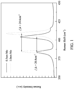
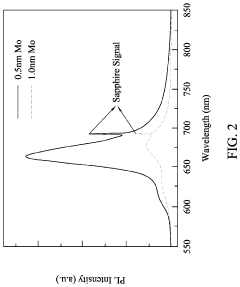
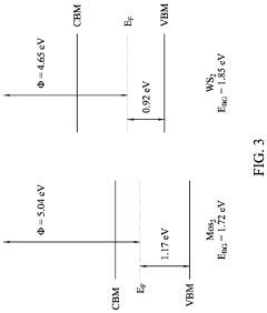
- The development of 2D crystal hetero-structures, specifically WS2/MoS2 hetero-structures, is achieved through chemical vapor deposition or sulfurization, enabling type-II band alignment and increased electron concentration by injecting electrons from WS2 to MoS2, thereby enhancing field-effect mobility and photoluminescence intensity.
Two dimensional structure and semiconductor device including the two dimensional structure, and method of manufacturing the semiconductor device
PatentPendingKR1020230050987A
Innovation
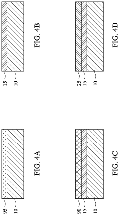
- A semiconductor device structure incorporating a first two-dimensional material layer with a single-layer structure and a second two-dimensional material layer with a multi-layer structure, formed on dielectric materials with varying defectivities, to enhance channel performance and reduce contact resistance.


Regulatory Harmonization Strategies
The global landscape of 2D semiconductor regulations presents significant challenges for industry stakeholders operating across multiple jurisdictions. Achieving regulatory harmonization requires strategic approaches that balance regional compliance requirements while maintaining operational efficiency. A comprehensive harmonization strategy must address the fragmented nature of current regulatory frameworks governing 2D semiconductor materials, manufacturing processes, and applications.
International standards organizations such as ISO, IEC, and IEEE have begun developing frameworks specifically for 2D semiconductor technologies, yet significant gaps remain between these emerging global standards and regional regulatory requirements. Companies must navigate this complex environment through systematic approaches that prioritize both compliance and innovation.
Key to successful harmonization is the establishment of cross-regional working groups that include industry representatives, regulatory bodies, and academic institutions. These collaborative forums can identify regulatory inconsistencies, propose unified testing methodologies, and develop consensus-based approaches to safety and performance standards. The International Electrotechnical Commission's Technical Committee 113 has made notable progress in this direction, though broader participation is needed.
Regulatory mapping represents another critical component of harmonization strategies. This involves creating comprehensive databases of jurisdiction-specific requirements for 2D semiconductor technologies, identifying overlaps and contradictions, and developing compliance pathways that satisfy multiple regulatory regimes simultaneously. Several multinational corporations have implemented such mapping systems internally, reducing redundant testing and certification processes.
Mutual recognition agreements (MRAs) between regulatory authorities offer significant potential for reducing compliance burdens. Current MRAs covering traditional semiconductor technologies could be expanded to explicitly include 2D materials and devices. The recent agreement between the EU and Japan regarding electronic equipment standards provides a potential template for such expansions.
Pre-competitive industry consortia focused on regulatory harmonization have demonstrated effectiveness in adjacent technology sectors. Similar initiatives for 2D semiconductors could accelerate the development of globally recognized test methods, safety protocols, and performance benchmarks. The formation of the 2D Semiconductor Global Alliance in 2022 represents a promising step in this direction, though its impact remains limited by insufficient participation from key Asian manufacturing hubs.
Ultimately, successful regulatory harmonization will require balanced approaches that respect legitimate regional differences while eliminating unnecessary regulatory divergence. Companies must engage proactively in standards development processes while simultaneously building flexible compliance systems capable of adapting to evolving regulatory landscapes.
International Trade Implications
The global trade landscape for 2D semiconductors is increasingly shaped by complex geopolitical tensions and strategic national interests. As countries recognize the critical importance of semiconductor technology for economic security and military applications, 2D semiconductor standards have become a focal point in international trade negotiations. The United States, European Union, Japan, and South Korea have formed strategic alliances to establish unified standards and secure supply chains, while simultaneously implementing export controls on advanced 2D semiconductor technologies to countries deemed security risks.
Trade barriers specifically targeting 2D semiconductor technologies have emerged in various forms, including tariffs, non-tariff barriers, and investment restrictions. These measures significantly impact global supply chains, with companies facing increased compliance costs and operational complexities. The semiconductor industry, historically built on global collaboration, now confronts fragmentation risks as nations pursue technological self-sufficiency through domestic manufacturing initiatives and protectionist policies.
Compliance with divergent national standards presents substantial challenges for multinational corporations operating in the 2D semiconductor space. Companies must navigate a complex web of regulations that often conflict across jurisdictions, requiring sophisticated compliance frameworks and region-specific product modifications. This regulatory fragmentation has accelerated the trend toward regionalized supply chains, with companies establishing parallel production capabilities in different markets to ensure uninterrupted access.
The World Trade Organization's role in mediating semiconductor trade disputes has diminished amid rising techno-nationalism, with bilateral and regional agreements increasingly governing semiconductor trade relations. The Comprehensive and Progressive Agreement for Trans-Pacific Partnership (CPTPP) and the EU-Japan Economic Partnership Agreement have incorporated specific provisions addressing semiconductor standards and intellectual property protection, establishing regional frameworks for 2D semiconductor trade.
Looking forward, international standardization bodies like the International Electrotechnical Commission (IEC) and IEEE are working to develop globally recognized standards for 2D semiconductor technologies. These efforts aim to reduce trade friction and facilitate market access while ensuring safety and interoperability. However, their success depends on balancing national security concerns with the benefits of open trade. Companies must develop adaptive strategies that anticipate regulatory shifts while maintaining compliance across multiple jurisdictions, potentially through modular product designs and diversified supply chains that can quickly adapt to changing trade requirements.
Unlock deeper insights with Patsnap Eureka Quick Research — get a full tech report to explore trends and direct your research. Try now!
Generate Your Research Report Instantly with AI Agent
Supercharge your innovation with Patsnap Eureka AI Agent Platform!