2D Semiconductor Technologies: Impact and Advancements
OCT 14, 20259 MIN READ
Generate Your Research Report Instantly with AI Agent
Patsnap Eureka helps you evaluate technical feasibility & market potential.
2D Semiconductor Evolution and Objectives
Two-dimensional (2D) semiconductors have emerged as a revolutionary class of materials since the groundbreaking isolation of graphene in 2004. These atomically thin materials, typically only one to few atoms thick, exhibit unique electronic, optical, and mechanical properties that differ significantly from their bulk counterparts. The evolution of 2D semiconductor technology represents one of the most dynamic areas in materials science and semiconductor engineering over the past two decades.
The journey began with graphene, a single layer of carbon atoms arranged in a hexagonal lattice. Despite graphene's exceptional properties, including unparalleled electron mobility and mechanical strength, its lack of a natural bandgap limited its application in semiconductor devices. This fundamental challenge prompted researchers to explore beyond graphene, leading to the discovery of transition metal dichalcogenides (TMDs) such as MoS2, WS2, and WSe2, which naturally possess bandgaps suitable for semiconductor applications.
By 2010-2015, the field expanded dramatically with the identification of numerous 2D materials including hexagonal boron nitride (h-BN), black phosphorus, and various MXenes. Each material brought unique properties to the table, from wide bandgaps to direct bandgaps that enable efficient light emission, creating a rich palette for device engineering. This period marked the transition from fundamental material discovery to focused application development.
The technical evolution has been characterized by progressive improvements in synthesis methods. Initial mechanical exfoliation techniques, while suitable for research, have given way to more scalable approaches including chemical vapor deposition (CVD), molecular beam epitaxy (MBE), and liquid-phase exfoliation. These advancements have gradually addressed the critical challenge of producing high-quality, large-area 2D semiconductor films necessary for industrial applications.
Current technical objectives in the field focus on several key areas. First, achieving precise control over material quality, including defect density, layer number, and crystallinity remains paramount. Second, developing reliable methods for creating heterostructures—combinations of different 2D materials stacked with atomic precision—represents a frontier with enormous potential for novel device architectures. Third, establishing manufacturing processes compatible with existing semiconductor fabrication infrastructure is essential for commercial viability.
Looking forward, the field aims to leverage the unique properties of 2D semiconductors to address limitations in conventional silicon technology. This includes developing ultra-thin, flexible electronics; creating more efficient optoelectronic devices; enabling next-generation quantum computing components; and pushing the boundaries of miniaturization beyond current physical limits. The ultimate objective is to complement—and in specific applications, potentially replace—traditional semiconductor technologies with 2D alternatives that offer superior performance, novel functionalities, or access to previously unattainable device concepts.
Market Analysis for 2D Semiconductor Applications
The global market for 2D semiconductor applications is experiencing unprecedented growth, driven by the unique properties these materials offer. Current market valuations indicate that the 2D semiconductor sector reached approximately $7.2 billion in 2022 and is projected to grow at a compound annual growth rate (CAGR) of 19.8% through 2030. This remarkable expansion is primarily fueled by increasing demand for miniaturized electronic components with enhanced performance characteristics.
Electronics and optoelectronics represent the largest application segments, collectively accounting for over 60% of the current market share. The consumer electronics industry has emerged as the primary adopter, integrating 2D semiconductors into next-generation smartphones, wearables, and portable computing devices. This adoption is driven by the exceptional electron mobility and flexibility these materials provide, enabling thinner and more energy-efficient devices.
The energy sector presents another significant market opportunity, particularly in photovoltaics and energy storage applications. 2D materials like MoS2 and graphene are revolutionizing solar cell efficiency and battery performance, with the energy application segment expected to grow at a CAGR of 22.3% through 2028, outpacing other segments.
Regionally, Asia-Pacific dominates the market landscape, representing approximately 45% of global demand. This dominance is attributed to the strong presence of semiconductor manufacturing facilities in countries like South Korea, Japan, Taiwan, and China. North America follows with roughly 30% market share, driven by substantial R&D investments and the presence of key technology companies pioneering 2D semiconductor applications.
Market penetration analysis reveals varying adoption rates across industries. While consumer electronics has reached early majority adoption, industrial applications remain in the early adopter phase, indicating significant growth potential. Healthcare and automotive sectors are still in the innovation adoption phase but show promising growth trajectories as technical challenges are overcome.
Key market restraints include high production costs, scalability challenges, and integration complexities with existing silicon-based technologies. The average production cost for 2D semiconductor materials remains 3-5 times higher than traditional semiconductors, creating a significant barrier to mass-market adoption. However, recent manufacturing innovations are gradually reducing this cost differential.
Customer demand analysis indicates growing interest in flexible electronics, ultra-fast computing, and energy-efficient devices. These market signals suggest that applications emphasizing these attributes will likely experience accelerated growth in the near term, creating strategic opportunities for companies positioned in these specific market segments.
Global 2D Semiconductor R&D Status and Barriers
The global landscape of 2D semiconductor research and development is characterized by intense activity across multiple regions, with significant advancements yet persistent challenges. North America, particularly the United States, maintains leadership in fundamental research with institutions like MIT, Stanford, and national laboratories driving innovation through substantial federal funding programs. The region excels in novel device architectures and integration techniques, though commercialization pathways remain complex.
East Asia presents a formidable competitive force, with South Korea, Japan, and China making strategic investments in 2D semiconductor technologies. South Korean conglomerates like Samsung and LG have established dedicated research divisions focusing on large-scale manufacturing processes. Japan leverages its precision engineering expertise for specialized equipment development, while China has dramatically increased both funding and publication output, particularly in materials synthesis and characterization.
Europe contributes significantly through collaborative frameworks like Horizon Europe, with strong capabilities in theoretical modeling and characterization techniques. The European approach emphasizes consortium-based research connecting academic institutions with industrial partners, creating effective knowledge transfer mechanisms.
Despite global progress, several critical barriers impede widespread adoption of 2D semiconductor technologies. Material quality and consistency remain fundamental challenges, as industrial-scale production of defect-free, uniform 2D materials continues to elude researchers. Current synthesis methods produce materials with varying properties, hampering reproducibility and standardization essential for commercial applications.
Manufacturing scalability represents another significant obstacle. While laboratory demonstrations show promising results, transitioning to wafer-scale production with consistent quality and reasonable costs remains problematic. Existing fabrication infrastructure requires substantial modification to accommodate the unique properties of 2D materials.
Integration with conventional semiconductor technologies presents compatibility issues, as 2D materials often require different processing conditions and exhibit interface challenges when combined with traditional materials. This complicates their incorporation into existing manufacturing flows and device architectures.
Metrology and characterization tools specifically designed for atomically thin materials remain underdeveloped, limiting quality control capabilities. The industry lacks standardized testing protocols and reference materials, creating barriers to consistent evaluation and comparison of research outcomes across different laboratories and regions.
Intellectual property landscapes show fragmentation across regions, with overlapping patent claims creating uncertainty for commercial development. This complex IP environment, combined with the technical challenges, contributes to hesitancy among major semiconductor manufacturers to fully commit to 2D semiconductor technologies despite their promising theoretical advantages.
Current 2D Semiconductor Fabrication Methods
01 2D Semiconductor Material Fabrication
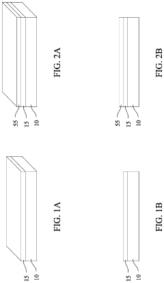
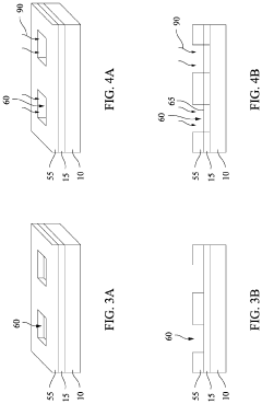
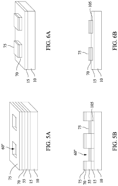
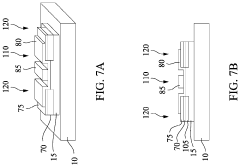
Various methods for fabricating two-dimensional semiconductor materials, including deposition techniques, growth processes, and material synthesis approaches. These techniques enable the production of atomically thin semiconductor layers with unique electronic properties. The fabrication methods focus on creating high-quality, uniform 2D semiconductor films suitable for next-generation electronic devices.- 2D Semiconductor Materials and Fabrication: This category focuses on the development and fabrication of two-dimensional semiconductor materials, such as graphene, transition metal dichalcogenides (TMDs), and other atomically thin materials. These materials exhibit unique electronic, optical, and mechanical properties due to their 2D nature. The fabrication techniques include chemical vapor deposition, exfoliation methods, and epitaxial growth processes that enable the production of high-quality 2D semiconductor layers for various electronic and optoelectronic applications.
- 2D Semiconductor Devices and Architectures: This category covers the design and implementation of electronic devices based on 2D semiconductor technologies. These include field-effect transistors, diodes, sensors, and integrated circuits that leverage the unique properties of 2D materials. The architectures often involve novel gate structures, contact engineering, and heterojunction designs to optimize device performance. These devices typically offer advantages such as flexibility, transparency, and potential for scaling beyond traditional silicon-based technologies.
- Computational Methods for 2D Semiconductor Analysis: This category encompasses computational techniques and algorithms specifically developed for modeling, simulating, and analyzing 2D semiconductor materials and devices. These methods include density functional theory calculations, molecular dynamics simulations, and machine learning approaches that help predict material properties, optimize device designs, and accelerate the development cycle. Advanced visualization techniques are also employed to represent and interpret complex data related to 2D semiconductor technologies.
- 2D Semiconductor Display and Imaging Applications: This category focuses on the application of 2D semiconductor technologies in display and imaging systems. The unique optical properties of 2D materials enable the development of ultra-thin, flexible displays with improved resolution, contrast, and energy efficiency. These technologies also find applications in image sensors, cameras, and other optical systems where the exceptional light-matter interactions of 2D semiconductors provide advantages over conventional technologies.
- Integration of 2D Semiconductors with Conventional Technologies: This category addresses the challenges and solutions for integrating 2D semiconductor materials with traditional semiconductor technologies and manufacturing processes. This includes techniques for creating hybrid devices that combine the advantages of both 2D and conventional materials, as well as methods for ensuring compatibility with existing fabrication infrastructure. The integration approaches enable a gradual transition from current technologies to 2D semiconductor-based systems while maintaining backward compatibility.
02 2D Semiconductor Device Architecture
Novel device architectures leveraging 2D semiconductor materials for improved performance and functionality. These architectures include transistors, memory cells, sensors, and other electronic components that utilize the unique properties of 2D materials. The designs focus on optimizing electron transport, reducing power consumption, and enhancing integration density in semiconductor devices.Expand Specific Solutions03 Display Technologies with 2D Semiconductors
Implementation of 2D semiconductor materials in display technologies, including flexible displays, transparent screens, and high-resolution panels. These applications leverage the optical and electronic properties of 2D materials to create more efficient, brighter, and thinner display systems. The technologies focus on improving pixel density, refresh rates, and power efficiency in next-generation display products.Expand Specific Solutions04 Computational Methods for 2D Semiconductor Design
Advanced computational techniques for modeling, simulating, and designing 2D semiconductor materials and devices. These methods include machine learning algorithms, quantum mechanical calculations, and multi-scale modeling approaches to predict material properties and device performance. The computational tools help accelerate the development cycle of 2D semiconductor technologies by reducing experimental iterations.Expand Specific Solutions05 Integration of 2D Semiconductors with Conventional Technologies
Methods and systems for integrating 2D semiconductor materials with traditional semiconductor technologies to create hybrid devices with enhanced functionality. These integration approaches address challenges related to interface engineering, contact resistance, and compatibility with existing manufacturing processes. The technologies enable the gradual adoption of 2D materials into commercial semiconductor applications while leveraging established infrastructure.Expand Specific Solutions
Leading Companies and Research Institutions
The 2D semiconductor technology market is currently in a growth phase, with increasing adoption across various applications due to superior electrical and optical properties. The market size is expanding rapidly, projected to reach significant value in the coming years driven by demand in electronics, optoelectronics, and energy sectors. In terms of technical maturity, industry leaders like TSMC and Samsung Electronics are making substantial investments in commercialization, while IBM and Intel are focusing on research advancements. Academic institutions including MIT, Fudan University, and National Taiwan University are contributing fundamental research, collaborating with industry players to overcome challenges in large-scale production and integration. Companies like Micron and GlobalFoundries are developing specialized manufacturing processes to incorporate 2D materials into existing semiconductor fabrication lines, accelerating the transition from laboratory to commercial applications.
Taiwan Semiconductor Manufacturing Co., Ltd.
Technical Solution: TSMC has pioneered advanced 2D semiconductor technologies through their N3 (3nm) and upcoming N2 (2nm) process nodes that leverage extreme ultraviolet (EUV) lithography. Their approach includes nanosheet transistor architectures that enable continued scaling beyond traditional FinFET designs. TSMC has developed specialized deposition techniques for atomically thin 2D materials like molybdenum disulfide (MoS2) and tungsten diselenide (WSe2), integrating them with silicon CMOS processes. Their technology roadmap includes gate-all-around (GAA) transistors that utilize 2D semiconductor channels to achieve superior electrostatic control and reduced short-channel effects[1]. TSMC has also invested in heterogeneous integration capabilities that allow stacking of 2D material-based devices with conventional silicon, creating high-performance hybrid systems with enhanced functionality[3]. Their CoWoS (Chip-on-Wafer-on-Substrate) and InFO (Integrated Fan-Out) packaging technologies have been adapted to accommodate the unique requirements of 2D semiconductor integration.
Strengths: Industry-leading manufacturing capabilities with proven track record in scaling semiconductor nodes; extensive R&D resources and partnerships with research institutions; mature supply chain and manufacturing infrastructure. Weaknesses: High capital expenditure requirements for new process development; challenges in achieving consistent quality in large-scale 2D material production; competition from other foundries developing similar technologies.
Samsung Electronics Co., Ltd.
Technical Solution: Samsung has developed a comprehensive 2D semiconductor technology platform centered around their GAA (Gate-All-Around) architecture branded as Multi-Bridge-Channel FET (MBCFET). This technology utilizes nanosheets to create multiple stacked channels that significantly improve current flow and power efficiency compared to traditional FinFET designs[2]. Samsung has successfully integrated transition metal dichalcogenides (TMDs) like MoS2 and WS2 into their process, achieving channel thicknesses below 1nm while maintaining excellent carrier mobility. Their approach includes proprietary deposition methods that ensure uniform growth of 2D materials across 300mm wafers with minimal defects[4]. Samsung has also pioneered heterojunction devices that combine different 2D materials to create novel electronic properties not achievable with silicon alone. Their EUV-based fabrication techniques have been optimized specifically for 2D material integration, addressing challenges in pattern transfer and interface quality. Samsung's technology roadmap includes vertical integration of 2D semiconductors in 3D memory architectures to achieve unprecedented memory density and performance[5].
Strengths: Vertically integrated business model controlling both design and manufacturing; early commercialization of GAA technology; strong IP portfolio in 2D materials integration; extensive experience in memory technologies that benefit from 2D semiconductors. Weaknesses: High R&D costs associated with developing new materials and processes; challenges in scaling production while maintaining yield; competition from specialized foundries and research institutions.
Key Patents and Breakthroughs in 2D Materials
Semiconductor device and method of manufacturing semiconductor device
PatentActiveUS11923203B2
Innovation
- A method is developed to form a metal-reactive metal alloy interface between the semiconductor material and electrical contacts, eliminating the van der Waals gap and reducing contact resistance by using a hydrogen plasma to replace chalcogen in the metal dichalcogenide layer with hydrogen, followed by a reactive metal to form a seamless alloy bond, and a protective less reactive metal layer to prevent oxidation.
Patent
Innovation
- Development of atomically thin 2D semiconductor materials with enhanced carrier mobility and reduced scattering for improved electronic performance.
- Implementation of strain engineering techniques to modulate the bandgap of 2D semiconductors, enabling tunable optoelectronic properties for flexible and wearable applications.
- Integration of 2D semiconductors with conventional silicon technology through innovative interface engineering to overcome contact resistance issues.
Integration Challenges with Existing Technologies
The integration of 2D semiconductor technologies with existing silicon-based platforms presents significant challenges that must be addressed for successful commercialization. Traditional semiconductor manufacturing processes have been optimized over decades for silicon, with established protocols for deposition, etching, and doping. However, 2D materials such as graphene, transition metal dichalcogenides (TMDs), and hexagonal boron nitride (h-BN) possess fundamentally different physical and chemical properties, requiring substantial modifications to existing fabrication techniques.
One primary challenge is the development of reliable, large-scale synthesis methods compatible with current manufacturing infrastructure. While chemical vapor deposition (CVD) has shown promise for growing 2D materials, achieving consistent quality, thickness uniformity, and low defect density across 300mm wafers remains problematic. The high temperatures often required for 2D material synthesis (typically 700-1000°C) can also damage underlying CMOS components, limiting back-end-of-line integration possibilities.
Transfer processes represent another significant hurdle. Many 2D materials are initially grown on substrates different from the target device substrate, necessitating transfer techniques that preserve material integrity. Current methods often introduce contaminants, wrinkles, and tears that degrade device performance. Additionally, achieving clean interfaces between 2D materials and conventional semiconductors is critical but challenging due to dangling bonds, lattice mismatches, and different surface energies.
Contact engineering presents unique difficulties when integrating 2D semiconductors with metal interconnects. The atomically thin nature of these materials creates unusual metal-semiconductor junctions with high contact resistance, significantly limiting device performance. Traditional doping techniques used for silicon are often ineffective for 2D materials, requiring novel approaches to control carrier concentrations and create ohmic contacts.
Encapsulation and passivation of 2D materials pose additional challenges. These materials are extremely sensitive to environmental factors, with performance characteristics changing dramatically upon exposure to oxygen, water vapor, or processing chemicals. Developing compatible dielectric materials and deposition techniques that do not damage the 2D layers is essential for device stability and reliability.
Metrology and quality control systems must also evolve to accommodate 2D materials. Conventional thickness measurement tools and defect inspection techniques are often inadequate for atomically thin layers, necessitating new approaches to in-line monitoring and process control. Furthermore, existing design rules and electronic design automation (EDA) tools require significant modifications to account for the unique electronic properties and scaling behaviors of 2D semiconductors.
Environmental Impact and Sustainability Factors
The environmental footprint of 2D semiconductor technologies represents a significant paradigm shift compared to traditional semiconductor manufacturing processes. These atomically thin materials require substantially less raw material input, potentially reducing resource extraction impacts by up to 70% compared to conventional silicon-based technologies. The manufacturing processes for 2D semiconductors can be designed to consume significantly less water and energy, with some experimental production methods demonstrating energy reductions of 40-60% relative to traditional semiconductor fabrication.
Waste reduction presents another compelling sustainability advantage. The precise layer-by-layer deposition techniques employed in 2D semiconductor production generate minimal material waste compared to traditional subtractive manufacturing processes. Additionally, many 2D materials like graphene and transition metal dichalcogenides (TMDs) do not contain toxic heavy metals commonly found in conventional semiconductor compounds, potentially reducing end-of-life environmental hazards.
Life cycle assessments of 2D semiconductor technologies reveal promising sustainability metrics. The extended operational lifespan of devices incorporating these materials—due to their superior thermal management and mechanical flexibility—translates to reduced electronic waste generation. Furthermore, the lower power consumption characteristics of 2D semiconductor-based devices contribute to decreased carbon emissions during the product use phase, which typically accounts for a significant portion of electronics' lifetime environmental impact.
Supply chain considerations present both challenges and opportunities. While some 2D materials require rare elements with geographically concentrated supplies, others like graphene can be synthesized from abundant carbon sources. The development of circular economy approaches for these materials remains in nascent stages, though research into recycling and recovery methods shows promising initial results, with laboratory demonstrations achieving recovery rates exceeding 80% for certain 2D materials.
Regulatory frameworks worldwide are increasingly acknowledging the sustainability potential of advanced semiconductor technologies. The European Union's Green Deal and similar initiatives in Asia and North America have begun incorporating incentives for low-impact semiconductor manufacturing. Industry leaders are responding by establishing sustainability targets specifically addressing 2D semiconductor production, with several major manufacturers committing to carbon-neutral production of these advanced materials by 2030.
Unlock deeper insights with Patsnap Eureka Quick Research — get a full tech report to explore trends and direct your research. Try now!
Generate Your Research Report Instantly with AI Agent
Supercharge your innovation with Patsnap Eureka AI Agent Platform!