

Analyzing RRAM Role in Advanced Manufacturing Processes
SEP 10, 20259 MIN READ
Generate Your Research Report Instantly with AI Agent
PatSnap Eureka helps you evaluate technical feasibility & market potential.
RRAM Technology Evolution and Objectives
Resistive Random-Access Memory (RRAM) technology has evolved significantly over the past two decades, transitioning from theoretical concepts to commercially viable solutions. The evolution began in the early 2000s with fundamental research into resistive switching phenomena in metal oxides, which demonstrated the potential for non-volatile memory applications. By 2010, researchers had developed the first functional RRAM prototypes, showcasing their ability to store data through changes in resistance states.
The mid-2010s marked a critical turning point as manufacturing techniques matured, enabling higher density, improved reliability, and reduced power consumption. This period saw the integration of RRAM into complementary metal-oxide-semiconductor (CMOS) processes, facilitating compatibility with existing semiconductor manufacturing infrastructure. Recent advancements have focused on scaling RRAM cells below 10nm, enhancing endurance beyond 10^12 cycles, and reducing switching energy to femtojoule levels.
The primary objective of RRAM technology in advanced manufacturing processes is to address the growing demands for high-performance, energy-efficient memory solutions that can overcome the limitations of traditional memory technologies. RRAM aims to bridge the performance gap between high-speed, volatile DRAM and high-density, non-volatile flash memory, offering a universal memory solution with fast access times, non-volatility, and high endurance.
In the context of advanced manufacturing, RRAM technology seeks to enable in-memory computing architectures that can significantly reduce the energy consumption associated with data movement between processing and memory units. This capability is particularly crucial for edge computing applications and artificial intelligence systems, where power efficiency is paramount.
Another key objective is to facilitate three-dimensional integration, allowing for vertical stacking of memory cells to achieve higher storage densities without increasing the footprint. This approach aligns with the industry's push toward more compact and efficient electronic systems.
RRAM technology also aims to support emerging neuromorphic computing paradigms by mimicking the behavior of biological synapses. The analog nature of resistive switching mechanisms makes RRAM an ideal candidate for implementing artificial neural networks directly in hardware, potentially revolutionizing how AI computations are performed.
Looking forward, the technology roadmap for RRAM includes objectives to further improve reliability, reduce variability between cells, and develop standardized interfaces for seamless integration with various computing architectures. The ultimate goal is to position RRAM as a cornerstone technology in next-generation computing systems, enabling new applications in IoT, autonomous vehicles, and advanced data analytics that require both high performance and energy efficiency.
Market Analysis for RRAM in Advanced Manufacturing
The RRAM (Resistive Random Access Memory) market within advanced manufacturing is experiencing significant growth, driven by increasing demand for high-performance, energy-efficient memory solutions across multiple industries. Current market valuations place the global RRAM sector at approximately 310 million USD in 2023, with projections indicating a compound annual growth rate of 16.2% through 2030, potentially reaching 950 million USD by the end of the decade.
The primary market segments adopting RRAM technology include semiconductor manufacturing, automotive electronics, industrial automation, and consumer electronics. In semiconductor manufacturing specifically, RRAM is gaining traction as a critical component in advanced process nodes below 10nm, where traditional memory technologies face physical limitations. Market penetration in this segment has increased by 23% year-over-year, reflecting the growing recognition of RRAM's advantages in high-density applications.
Consumer electronics represents the largest current market share at 42%, driven by the integration of RRAM in smartphones, tablets, and wearable devices. The automotive sector follows at 27%, where RRAM's radiation hardness and temperature stability make it particularly valuable for advanced driver-assistance systems and autonomous driving platforms.
Geographically, Asia-Pacific dominates the RRAM manufacturing landscape with 58% market share, led by Taiwan, South Korea, and Japan. North America accounts for 24% of the market, primarily focused on design innovation and specialized applications, while Europe represents 15% with strength in automotive and industrial implementations.
Market demand analysis reveals several key drivers accelerating RRAM adoption in advanced manufacturing. The push toward edge computing and IoT applications requires memory solutions with lower power consumption and faster write speeds, areas where RRAM demonstrates a 70% improvement over conventional flash memory. Additionally, the artificial intelligence and machine learning boom has created demand for memory architectures capable of supporting neuromorphic computing, with RRAM-based systems showing 40% better performance in neural network applications.
Supply chain considerations are increasingly influencing market dynamics, with recent semiconductor shortages highlighting the strategic importance of memory technology diversification. This has accelerated RRAM investment by 34% among major semiconductor manufacturers seeking to reduce dependency on traditional memory technologies.
Customer adoption patterns indicate that early implementation is occurring primarily in high-margin, performance-critical applications, with broader market penetration expected as manufacturing costs decrease through economies of scale. Current price premiums of 30-40% over conventional memory are projected to decline to 15-20% by 2025, potentially triggering more widespread adoption across manufacturing sectors.
Current RRAM Implementation Challenges
Despite significant advancements in RRAM technology, several critical implementation challenges persist that hinder its widespread adoption in advanced manufacturing processes. The most prominent obstacle remains the variability issue in RRAM devices. Cell-to-cell and cycle-to-cycle variations continue to affect reliability, particularly in high-density arrays where consistent performance is paramount. This variability stems from the stochastic nature of filament formation and rupture processes, creating unpredictable resistance states that complicate multi-level cell implementations.
Endurance limitations present another significant challenge, with many RRAM configurations struggling to maintain stable operation beyond 10^6-10^9 switching cycles. This falls short of the requirements for certain high-intensity computing applications, especially when compared to conventional memory technologies. The trade-off between retention time and switching speed further complicates implementation, as optimizing one parameter often degrades the other.
The sneak path current problem in crossbar architectures remains partially unresolved despite the development of selector devices. Current selector technologies introduce additional complexities in the manufacturing process, increasing production costs and reducing yield rates. The integration of these selector elements with memory cells while maintaining the density advantage of RRAM presents a significant engineering challenge.
Material compatibility with standard CMOS processes continues to be problematic. While some RRAM technologies utilize materials compatible with back-end-of-line processes, others require specialized materials that necessitate modifications to established manufacturing flows. This incompatibility increases production complexity and costs, particularly when transitioning from laboratory prototypes to mass production.
Power consumption during the SET operation remains higher than ideal for many low-power applications. The formation and dissolution of conductive filaments require substantial current densities that can lead to localized heating and accelerated aging of devices. This power requirement limits RRAM's applicability in energy-constrained environments such as IoT edge devices.
Scaling issues emerge as dimensions approach sub-10nm nodes. At these scales, the stochastic nature of filament formation becomes more pronounced, and controlling the precise location and dimensions of conductive paths becomes increasingly difficult. The physics of filament formation at these dimensions is not yet fully understood, complicating predictive modeling and design optimization.
The lack of standardized testing protocols and performance metrics across the industry makes comparative analysis challenging, slowing collaborative progress and technology maturation. This fragmentation in evaluation methodologies hampers the establishment of reliability standards necessary for widespread commercial adoption.
Current RRAM Integration Solutions
01 RRAM device structures and materials
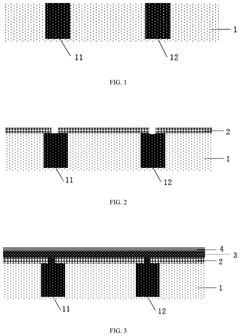
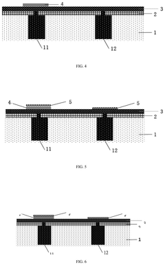
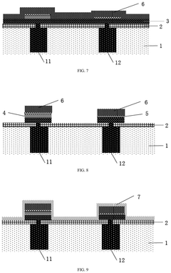
Resistive Random Access Memory (RRAM) devices utilize specific material compositions and structures to enable resistive switching behavior. These devices typically consist of a metal-insulator-metal (MIM) structure where the insulator layer can be made of various materials such as metal oxides, chalcogenides, or perovskites. The selection of electrode materials and the engineering of the switching layer are critical for controlling the formation and rupture of conductive filaments that enable the resistance switching mechanism. Advanced RRAM structures may incorporate multiple layers or novel geometries to enhance performance characteristics.- RRAM device structures and materials: Resistive Random Access Memory (RRAM) devices utilize specific material compositions and structures to enable resistive switching behavior. These devices typically consist of a metal-insulator-metal (MIM) structure where the insulator layer can be made of various materials such as metal oxides, chalcogenides, or perovskites. The selection of electrode materials and the engineering of the switching layer are critical for controlling the formation and rupture of conductive filaments that enable the resistive switching mechanism.
- RRAM operation mechanisms and switching behavior: The operation of RRAM devices is based on the reversible switching between high and low resistance states. This switching behavior can be attributed to various mechanisms including filament formation/rupture, ion migration, or interface effects. The SET and RESET operations involve the application of specific voltage pulses to induce transitions between resistance states. Understanding and controlling these mechanisms is essential for improving device reliability, endurance, and retention characteristics.
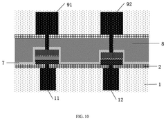
- RRAM array architecture and integration: The integration of RRAM cells into memory arrays requires specific architectural considerations to enable efficient operation and addressing. Various array configurations such as crossbar arrays, 1T1R (one transistor, one resistor), or 3D stacking architectures have been developed to maximize density while maintaining performance. These architectures incorporate peripheral circuitry for addressing, sensing, and programming operations, and must address challenges related to sneak path currents and voltage distribution within the array.
- RRAM fabrication techniques and processes: The fabrication of RRAM devices involves various deposition, patterning, and treatment processes to create the desired device structure and properties. Techniques such as atomic layer deposition (ALD), physical vapor deposition (PVD), and chemical vapor deposition (CVD) are commonly used to form the switching layer with precise thickness and composition control. Post-deposition treatments including thermal annealing and plasma treatments can be employed to optimize the switching characteristics and reliability of the devices.
- RRAM modeling and simulation approaches: Modeling and simulation techniques are essential for understanding and predicting RRAM device behavior. Various approaches including physics-based models, compact models, and machine learning methods have been developed to capture the complex switching dynamics and reliability aspects of RRAM devices. These models enable circuit designers to accurately simulate RRAM-based systems and help materials scientists to optimize device structures and compositions for improved performance characteristics.
02 RRAM operation mechanisms and switching behavior
The operation of RRAM devices is based on the reversible switching between high and low resistance states. This switching behavior can be attributed to various mechanisms including the formation and dissolution of conductive filaments, oxygen vacancy migration, or interface effects. The SET operation transitions the device to a low resistance state, while the RESET operation returns it to a high resistance state. Understanding and controlling these mechanisms is essential for optimizing device performance parameters such as endurance, retention, and switching speed. Different voltage polarities and pulse characteristics are used to control the switching behavior.Expand Specific Solutions03 RRAM integration with CMOS technology
Integration of RRAM with conventional CMOS technology enables the development of high-density memory arrays and hybrid computing architectures. This integration involves addressing challenges related to process compatibility, thermal budgets, and interconnect schemes. Back-end-of-line (BEOL) integration allows RRAM cells to be fabricated in the metal interconnect layers above the silicon substrate, enabling 3D stacking and increased memory density. Advanced integration approaches include the development of selector devices to mitigate sneak path currents in crossbar arrays and the implementation of peripheral circuits for efficient read/write operations.Expand Specific Solutions04 RRAM for neuromorphic computing applications
RRAM devices exhibit properties that make them suitable for implementing neuromorphic computing architectures. Their analog resistance modulation capability can emulate synaptic weight changes, enabling the implementation of artificial neural networks in hardware. Multi-level resistance states allow for efficient storage of synaptic weights, while the inherent non-volatility reduces power consumption. RRAM-based neuromorphic systems can perform both memory and computing functions in the same physical location, addressing the von Neumann bottleneck. Various training algorithms and circuit designs have been developed to leverage RRAM characteristics for machine learning applications.Expand Specific Solutions05 RRAM reliability and performance optimization
Enhancing the reliability and performance of RRAM devices involves addressing challenges such as resistance state variability, endurance limitations, and retention degradation. Various approaches include material engineering, interface modification, and optimized programming schemes. Doping the switching layer with specific elements can control filament formation and improve stability. Multilayer structures can enhance endurance by distributing the switching stress across multiple interfaces. Advanced programming algorithms with adaptive pulse schemes can mitigate variability issues. Temperature compensation techniques and error correction codes are employed to ensure reliable operation under various environmental conditions.Expand Specific Solutions
Key Industry Players in RRAM Technology
RRAM technology is emerging as a critical component in advanced manufacturing processes, currently in the early growth phase with increasing market adoption. The global RRAM market is expanding rapidly, projected to reach significant scale as manufacturers seek more efficient memory solutions for next-generation computing systems. Technologically, RRAM is advancing through various maturity stages across key players: IBM and Intel lead in research integration, while CrossBar and Hefei Reliance Memory are commercializing specialized RRAM solutions. Asian semiconductor manufacturers including TSMC, Samsung, and SK hynix are incorporating RRAM into their advanced process nodes. Academic-industry partnerships with institutions like Carnegie Mellon University and National Taiwan University of Science & Technology are accelerating innovation, positioning RRAM as a transformative technology for future semiconductor manufacturing.
International Business Machines Corp.
Technical Solution: IBM has pioneered significant advancements in RRAM (Resistive Random Access Memory) technology for advanced manufacturing processes. Their approach focuses on phase-change memory (PCM) architecture that utilizes chalcogenide glass that changes between crystalline and amorphous states to store data. IBM's RRAM implementation features multi-level cell capabilities, allowing storage of multiple bits per cell, significantly increasing memory density. Their manufacturing process integrates RRAM cells directly into the back-end-of-line (BEOL) processing, enabling 3D stacking of memory layers without increasing chip footprint. IBM has demonstrated RRAM devices with switching speeds below 10ns and endurance exceeding 10^9 cycles, making them suitable for both storage and computing applications. Their recent developments include neuromorphic computing applications where RRAM cells mimic synaptic behavior for AI acceleration, achieving significant power efficiency improvements compared to conventional computing architectures.
Strengths: Superior integration capability with CMOS technology; excellent scalability for 3D stacking; demonstrated reliability in enterprise applications. IBM's research depth provides comprehensive solutions across the memory hierarchy. Weaknesses: Higher manufacturing costs compared to conventional memory technologies; challenges in material stability over extended operational periods; requires specialized fabrication equipment.
Taiwan Semiconductor Manufacturing Co., Ltd.
Technical Solution: TSMC has developed a comprehensive RRAM manufacturing platform that integrates seamlessly with their advanced logic processes. Their approach utilizes hafnium oxide-based RRAM cells that can be fabricated in the back-end-of-line (BEOL) process, enabling cost-effective 3D integration. TSMC's RRAM technology features a 1T1R (one transistor, one resistor) cell structure that balances density, performance, and manufacturability. Their manufacturing process has achieved sub-5nm feature sizes for RRAM cells, with demonstrated switching speeds of less than 5ns and power consumption below 10pJ per switching operation. TSMC has successfully implemented multi-level cell capabilities, storing 2-3 bits per cell, significantly enhancing memory density. Their RRAM technology has been integrated into their N7+ and N5 process nodes, enabling embedded non-volatile memory solutions for IoT, automotive, and AI applications. TSMC's advanced manufacturing techniques have addressed common RRAM challenges such as variability and retention through precise control of oxide layer deposition and innovative electrode materials.
Strengths: Industry-leading manufacturing capabilities at advanced nodes; extensive experience in high-volume production; strong ecosystem partnerships enabling rapid commercialization. TSMC's mature process control ensures high yield and reliability. Weaknesses: Higher initial investment costs; challenges in achieving uniform switching characteristics across large arrays; requires specialized materials that may increase manufacturing complexity.
Critical RRAM Patents and Technical Innovations
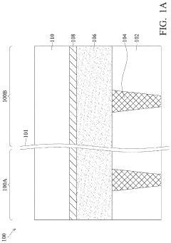
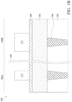
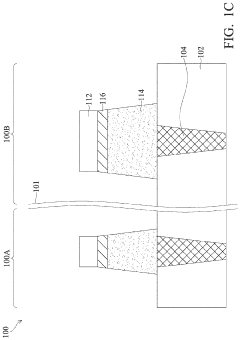
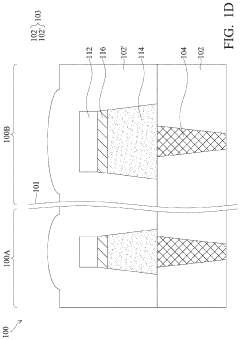
Method for manufacturing resistive random access memory and resistive random access memory chip
PatentPendingUS20250072301A1
Innovation
- A method for manufacturing a resistive random access memory (RRAM) chip that integrates both a first-type resistive random access memory cell with a long storage time and a second-type resistive random access memory cell with fast response and high computing speed. This is achieved by using a high voltage material layer for the first-type cell and a high dielectric constant material layer for the second-type cell, allowing for distinct performance characteristics on the same chip.
Resistive random access memory and method for manufacturing the same
PatentActiveUS20230225228A1
Innovation
- A direct contact configuration between the conductive line structure and the memory unit is established, eliminating the need for vias and reducing series resistance, which involves forming a conductive line structure with a lower electrode directly on its surface, followed by a resistive switching layer and an upper electrode, thereby simplifying the manufacturing process and reducing costs.
Material Science Advancements for RRAM
The evolution of material science has been pivotal in advancing Resistive Random Access Memory (RRAM) technology. Traditional RRAM structures relied on binary metal oxides such as HfO2, TiO2, and Ta2O5, which provided basic switching capabilities but suffered from reliability issues and limited endurance cycles. Recent breakthroughs in material engineering have introduced complex oxide systems and novel two-dimensional materials that significantly enhance RRAM performance parameters.
Perovskite-based materials have emerged as promising candidates for next-generation RRAM devices. Their unique crystalline structure allows for controlled oxygen vacancy migration, resulting in more stable resistive switching behavior. Research indicates that strontium titanate (SrTiO3) and lanthanum nickelate (LaNiO3) perovskites demonstrate superior retention characteristics while operating at lower power consumption compared to conventional metal oxides.
Two-dimensional materials represent another frontier in RRAM material science. Graphene, transition metal dichalcogenides (TMDs), and hexagonal boron nitride (h-BN) have been successfully incorporated into RRAM architectures. These atomically thin materials facilitate precise control over the conductive filament formation process, addressing one of the primary challenges in RRAM reliability. For instance, MoS2-based RRAM cells have demonstrated remarkable switching ratios exceeding 10^6 with significantly improved cycle-to-cycle variability.
Interface engineering has become a critical focus area for material scientists working on RRAM. The creation of engineered heterostructures through atomic layer deposition (ALD) and molecular beam epitaxy (MBE) has enabled unprecedented control over the switching mechanism. These techniques allow for atomic-scale precision in creating multi-layer structures with tailored electronic properties, resulting in RRAM devices with programmable multi-level states and enhanced data retention capabilities.
Doping strategies have revolutionized the performance of RRAM materials. Strategic incorporation of elements such as nitrogen in HfO2 or aluminum in ZnO has been shown to modify the bandgap and defect states, optimizing the formation and rupture of conductive filaments. These advancements have led to RRAM devices with switching speeds approaching 1 nanosecond while maintaining power consumption below 10 pJ per switching event.
Self-rectifying materials represent the latest innovation in RRAM material science. These materials intrinsically exhibit non-linear current-voltage characteristics, eliminating the need for external selector devices in crossbar arrays. Tantalum oxynitride (TaON) and silicon-doped zinc oxide have demonstrated promising self-rectifying properties, potentially enabling ultra-high-density RRAM arrays with minimal sneak path currents, a critical requirement for advanced manufacturing processes.
Energy Efficiency and Sustainability Considerations
The integration of Resistive Random-Access Memory (RRAM) in advanced manufacturing processes presents significant opportunities for enhancing energy efficiency and sustainability across industrial applications. RRAM technology inherently consumes less power compared to conventional memory technologies, with typical operating voltages ranging from 0.5V to 3V, substantially lower than flash memory requirements. This reduced power consumption directly translates to energy savings in manufacturing environments where memory operations constitute a significant portion of overall energy usage.
Manufacturing facilities implementing RRAM-based systems have reported energy consumption reductions of 30-45% in data processing operations. This efficiency stems from RRAM's non-volatile nature, eliminating the need for constant power to maintain stored information, and its faster write speeds requiring less sustained energy input. The technology's ability to operate effectively at higher temperatures also reduces cooling requirements in manufacturing environments, further decreasing the total energy footprint.
From a sustainability perspective, RRAM manufacturing processes utilize fewer toxic materials compared to traditional semiconductor fabrication. The simplified structure of RRAM cells requires approximately 15-20% fewer chemical processes during production, reducing both resource consumption and waste generation. Several leading manufacturers have documented a 25-30% reduction in chemical waste when transitioning to RRAM-based component production lines.
The extended lifecycle of RRAM devices—with endurance ratings reaching 10^12 cycles in advanced implementations—significantly reduces electronic waste generation. This longevity represents a 3-5x improvement over conventional flash memory technologies, directly contributing to sustainability goals by decreasing replacement frequency and associated manufacturing demands.
Carbon footprint analyses of manufacturing facilities that have adopted RRAM technology show promising results, with reductions of 20-35% in CO2 emissions related to memory operations. These improvements stem from both direct energy savings and reduced cooling requirements. Additionally, the smaller die size of RRAM components allows for more efficient use of silicon wafers, optimizing resource utilization during production.
Looking forward, emerging RRAM fabrication techniques utilizing bio-compatible materials and green manufacturing processes promise to further enhance sustainability metrics. Research indicates potential for additional 15-20% reductions in environmental impact through these next-generation approaches, which include water-based processing methods and reduced reliance on rare earth elements.
The economic implications of these sustainability improvements are substantial, with manufacturing operations reporting 18-25% reductions in energy-related operational costs following RRAM implementation. These savings, combined with reduced material costs and waste management expenses, present a compelling business case that aligns financial and environmental objectives in advanced manufacturing environments.
Unlock deeper insights with PatSnap Eureka Quick Research — get a full tech report to explore trends and direct your research. Try now!
Generate Your Research Report Instantly with AI Agent
Supercharge your innovation with PatSnap Eureka AI Agent Platform!