

Optimizing RRAM Memory Capacity for High-Density Storage
SEP 10, 20259 MIN READ
Generate Your Research Report Instantly with AI Agent
PatSnap Eureka helps you evaluate technical feasibility & market potential.
RRAM Technology Evolution and Capacity Goals
Resistive Random Access Memory (RRAM) has emerged as a promising non-volatile memory technology over the past two decades, evolving from theoretical concepts to commercial applications. The technology leverages resistance switching phenomena in metal-oxide materials to store binary information, offering advantages in scalability, power consumption, and integration potential compared to conventional memory technologies. The evolution of RRAM has been marked by significant improvements in material engineering, device architecture, and fabrication processes.
Early RRAM development in the early 2000s focused primarily on proof-of-concept demonstrations with limited capacity and reliability. By 2010, research shifted toward understanding the fundamental switching mechanisms and improving device characteristics, achieving densities of approximately 4-8 Gb/cm². The period between 2015 and 2020 saw substantial progress in scaling, with some research prototypes demonstrating capacities approaching 32-64 Gb/cm².
Current technological goals for RRAM capacity optimization center on achieving ultra-high density storage exceeding 1 Tb/cm² while maintaining acceptable performance metrics. This ambitious target requires overcoming several fundamental limitations, including sneak path currents in crossbar arrays, variability in switching behavior, and endurance degradation at smaller feature sizes.
The capacity evolution trajectory follows a pattern similar to Moore's Law, with density doubling approximately every 18-24 months during periods of active development. However, this pace has slowed in recent years as fundamental physical limitations have become more prominent. Industry roadmaps project that RRAM technologies could potentially reach 256 Gb to 1 Tb per die within the next five years, contingent upon successful resolution of current technical challenges.
Material innovation represents a critical factor in capacity enhancement, with transition metal oxides like HfOx, TaOx, and TiOx showing particular promise for high-density applications. Multi-level cell (MLC) approaches, which store multiple bits per cell by utilizing intermediate resistance states, offer another pathway to increase effective storage density by 2-4x without proportional increases in physical cell count.
3D integration strategies, including vertical RRAM (VRRAM) and 3D crosspoint architectures, present perhaps the most promising avenue for dramatic capacity improvements. These approaches leverage the inherent simplicity of RRAM cells to create stacked memory arrays, potentially increasing capacity by an order of magnitude compared to planar implementations.
The ultimate capacity goals for RRAM technology aim to position it as a viable storage-class memory solution, bridging the performance gap between DRAM and NAND flash while offering superior density to the former and better performance than the latter.
Market Demand Analysis for High-Density Storage
The global demand for high-density storage solutions has experienced exponential growth in recent years, primarily driven by the proliferation of data-intensive applications across various sectors. The digital universe is expanding at an unprecedented rate, with global data creation projected to reach 175 zettabytes by 2025, representing a compound annual growth rate of approximately 27% from 2020. This massive data explosion necessitates storage technologies that can accommodate higher capacities while maintaining or reducing physical footprints.
RRAM (Resistive Random Access Memory) technology has emerged as a promising candidate to address these high-density storage requirements. Market research indicates that the RRAM market is expected to grow significantly, with projections suggesting a market value exceeding $4 billion by 2028. This growth is substantially higher than traditional memory technologies, reflecting the increasing recognition of RRAM's potential to revolutionize storage architectures.
Several key market segments are driving demand for optimized RRAM solutions. The enterprise data center market, facing challenges of space constraints and energy efficiency, represents a primary target. With data centers consuming approximately 1-2% of global electricity and growing, the need for high-density, energy-efficient storage solutions like optimized RRAM is critical. Industry reports suggest that data center operators could reduce storage-related energy consumption by up to 30% through next-generation memory technologies.
Consumer electronics constitutes another significant market segment, with smartphones, tablets, and wearable devices requiring increasingly compact yet powerful storage solutions. The average storage capacity in smartphones has increased from 32GB to over 256GB in just five years, highlighting the demand trajectory for high-density solutions that RRAM could address.
Emerging applications in edge computing and Internet of Things (IoT) present substantial growth opportunities for optimized RRAM. The number of connected IoT devices is expected to surpass 25 billion by 2030, each generating data that requires processing and storage. RRAM's characteristics make it particularly suitable for these distributed computing environments where power efficiency and form factor are crucial considerations.
Automotive and industrial sectors are also showing increased interest in high-density non-volatile memory solutions. Advanced driver-assistance systems (ADAS) and autonomous vehicles generate terabytes of data daily, creating demand for robust, high-capacity storage technologies. Similarly, industrial automation systems increasingly rely on local data processing and storage capabilities, representing another growth vector for optimized RRAM solutions.
RRAM Technical Challenges and Density Limitations
RRAM (Resistive Random Access Memory) technology faces significant technical challenges that currently limit its storage density capabilities. The fundamental challenge lies in the trade-off between cell size reduction and maintaining reliable performance. As cell dimensions shrink below 10nm, quantum tunneling effects and variability in switching behavior become increasingly problematic, causing inconsistent resistance states and reduced reliability.
Material interface issues present another major limitation. The metal-oxide interfaces in RRAM devices often suffer from defect formation and ion migration inconsistencies at nanoscale dimensions. These defects create unpredictable conductive filament formation, resulting in significant device-to-device and cycle-to-cycle variations that compromise storage density potential.
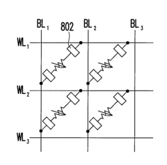
Sneak path currents represent a critical challenge in high-density crossbar arrays. Without proper selector devices, parasitic currents flow through unselected cells, causing read errors and increased power consumption. While various selector technologies have been proposed, integrating them without increasing cell area remains difficult, creating a fundamental density limitation.
The forming process required to initialize RRAM cells presents another obstacle. This high-voltage operation creates structural variations that lead to inconsistent switching behaviors across an array. As density increases, these variations become more pronounced, making it difficult to maintain uniform performance across billions of cells in high-capacity storage applications.
Endurance and retention characteristics deteriorate as cell dimensions decrease. Smaller cells contain fewer oxygen vacancies and conductive filaments with reduced stability, leading to faster degradation and shorter lifetimes. High-density implementations require cells to maintain performance through thousands of write cycles while retaining data for years, a requirement that becomes increasingly difficult to meet as dimensions shrink.
Manufacturing challenges further constrain density improvements. Current fabrication techniques struggle with precise control of oxide layer thickness and composition at nanoscale dimensions. Process variations lead to significant performance differences between cells, necessitating complex error correction mechanisms that consume additional chip area.
Heat dissipation becomes increasingly problematic as cell density increases. The resistive switching process generates significant localized heating that can affect neighboring cells in high-density arrays, causing data corruption or accelerated wear. Thermal management solutions typically require additional spacing between cells, directly limiting achievable density.
Material interface issues present another major limitation. The metal-oxide interfaces in RRAM devices often suffer from defect formation and ion migration inconsistencies at nanoscale dimensions. These defects create unpredictable conductive filament formation, resulting in significant device-to-device and cycle-to-cycle variations that compromise storage density potential.
Sneak path currents represent a critical challenge in high-density crossbar arrays. Without proper selector devices, parasitic currents flow through unselected cells, causing read errors and increased power consumption. While various selector technologies have been proposed, integrating them without increasing cell area remains difficult, creating a fundamental density limitation.
The forming process required to initialize RRAM cells presents another obstacle. This high-voltage operation creates structural variations that lead to inconsistent switching behaviors across an array. As density increases, these variations become more pronounced, making it difficult to maintain uniform performance across billions of cells in high-capacity storage applications.
Endurance and retention characteristics deteriorate as cell dimensions decrease. Smaller cells contain fewer oxygen vacancies and conductive filaments with reduced stability, leading to faster degradation and shorter lifetimes. High-density implementations require cells to maintain performance through thousands of write cycles while retaining data for years, a requirement that becomes increasingly difficult to meet as dimensions shrink.
Manufacturing challenges further constrain density improvements. Current fabrication techniques struggle with precise control of oxide layer thickness and composition at nanoscale dimensions. Process variations lead to significant performance differences between cells, necessitating complex error correction mechanisms that consume additional chip area.
Heat dissipation becomes increasingly problematic as cell density increases. The resistive switching process generates significant localized heating that can affect neighboring cells in high-density arrays, causing data corruption or accelerated wear. Thermal management solutions typically require additional spacing between cells, directly limiting achievable density.
Current High-Density RRAM Architectures
01 High-density RRAM architectures
Various architectural approaches are employed to increase RRAM memory capacity, including 3D stacking, crossbar arrays, and multi-level cell configurations. These designs allow for higher density memory integration while maintaining performance characteristics. Advanced fabrication techniques enable the creation of compact memory cells with reduced feature sizes, contributing to increased storage capacity in smaller physical footprints.- High-density RRAM architectures: RRAM technology enables high-density memory architectures through various structural innovations. These include 3D stacking, crossbar arrays, and multi-level cell configurations that significantly increase storage capacity within a small footprint. The vertical integration of memory cells allows for greater bit density compared to traditional memory technologies, making RRAM suitable for applications requiring large storage capacity in limited space.
- Multi-level cell (MLC) technology in RRAM: Multi-level cell technology in RRAM allows each memory cell to store multiple bits of information by utilizing different resistance states. This approach significantly increases memory capacity without increasing the physical size of the memory array. By precisely controlling the resistance levels in each cell, MLC RRAM can achieve higher storage density compared to single-bit-per-cell implementations, though it requires sophisticated programming and sensing circuits to distinguish between the multiple resistance states.
- Novel materials for enhanced RRAM capacity: Advanced materials play a crucial role in improving RRAM memory capacity. Various oxide-based materials, metal oxides, and novel switching materials are being developed to enhance the performance and reliability of RRAM cells. These materials enable better resistance switching characteristics, improved retention, and higher endurance, which collectively contribute to increased memory capacity and density. The selection of appropriate materials for the resistive switching layer is critical for optimizing memory capacity while maintaining reliability.
- Scaling and miniaturization techniques: Scaling and miniaturization techniques are essential for increasing RRAM memory capacity. These include reducing the physical dimensions of memory cells, optimizing electrode materials and configurations, and developing advanced fabrication processes. Nanoscale RRAM cells can be packed more densely on a chip, significantly increasing the overall memory capacity. Various approaches to scaling, such as reducing the thickness of the switching layer and minimizing electrode sizes, contribute to higher bit densities while maintaining reliable switching behavior.
- Integration with advanced control circuitry: Integration of RRAM with advanced control circuitry is crucial for maximizing memory capacity. Sophisticated sensing circuits, programming algorithms, and error correction techniques enable reliable operation of high-density RRAM arrays. These control systems allow for precise management of resistance states, mitigate variability issues, and enhance the overall capacity by ensuring reliable data storage and retrieval. Advanced addressing schemes and selector devices also contribute to increasing the effective memory capacity by enabling efficient access to individual cells in large arrays.
02 Multi-level cell technology for RRAM
Multi-level cell (MLC) technology enables RRAM devices to store multiple bits per cell by utilizing different resistance states. This approach significantly increases memory capacity without expanding the physical size of the memory array. By precisely controlling the resistance levels and developing sophisticated sensing circuits, RRAM devices can achieve higher bit density and storage capacity compared to conventional binary storage methods.Expand Specific Solutions03 Materials innovation for enhanced RRAM capacity
Novel materials and material combinations are being developed to enhance RRAM memory capacity. These include specialized metal oxides, phase change materials, and nanostructured composites that exhibit superior switching characteristics and reliability. Materials engineering at the nanoscale allows for more stable resistance states, better endurance, and higher storage density, directly contributing to increased memory capacity.Expand Specific Solutions04 Integration and scaling techniques for RRAM
Advanced integration techniques enable higher RRAM memory capacity through improved scaling and compatibility with existing semiconductor processes. These include back-end-of-line integration, vertical integration strategies, and novel selector device implementations. By optimizing the integration of RRAM cells with peripheral circuitry and addressing schemes, overall system capacity can be significantly increased while maintaining performance and power efficiency.Expand Specific Solutions05 System-level approaches for maximizing RRAM capacity
System-level innovations focus on maximizing effective RRAM memory capacity through advanced memory management, error correction, and hybrid memory architectures. These approaches include specialized controllers, wear-leveling algorithms, and integration with other memory technologies in hierarchical systems. By optimizing the entire memory subsystem around RRAM characteristics, these solutions achieve higher usable capacity and improved overall system performance.Expand Specific Solutions
Leading RRAM Technology Companies and Research Institutions
The RRAM memory optimization landscape is currently in a growth phase, with the market expanding as technology matures from research to commercialization. Major semiconductor players like Intel, Samsung, Micron, and TSMC are leading development efforts, with Intel and Samsung demonstrating the most advanced RRAM implementations for high-density storage. Academic institutions including Fudan University and Huazhong University of Science & Technology are contributing significant research breakthroughs. The technology is approaching commercial viability, with companies like Winbond and ChangXin Memory Technologies moving toward production-ready solutions. Qualcomm and Apple are exploring RRAM for mobile applications, while research institutes like ITRI are developing next-generation architectures to overcome current density limitations.
Intel Corp.
Technical Solution: Intel has developed a comprehensive RRAM optimization approach focusing on their 3D XPoint technology (developed with Micron). Their solution addresses high-density storage challenges through innovative cross-point architecture where memory cells are placed at the intersection of word lines and bit lines in a three-dimensional array. Intel's approach includes advanced selector devices to minimize sneak path currents, which traditionally limit array density. They've implemented multi-level cell (MLC) capabilities allowing each memory cell to store multiple bits, effectively doubling or quadrupling memory density without increasing physical cell count. Intel has also pioneered specialized write and read algorithms that compensate for cell-to-cell variations, enabling reliable operation at smaller technology nodes and higher densities[1]. Their recent developments include optimized forming processes that reduce the energy required for initial cell programming while improving long-term reliability.
Strengths: Industry-leading 3D integration expertise, established manufacturing infrastructure, and comprehensive ecosystem support. Their selector technology effectively addresses sneak path issues that typically limit array size. Weaknesses: Higher power consumption compared to emerging RRAM technologies, and their solutions often require more complex peripheral circuitry which can offset some density advantages.
Taiwan Semiconductor Manufacturing Co., Ltd.
Technical Solution: TSMC has developed specialized RRAM fabrication processes optimized for high-density storage applications. Their approach focuses on back-end-of-line (BEOL) integration, allowing RRAM arrays to be stacked above conventional CMOS logic, significantly increasing effective memory density without expanding chip footprint. TSMC's solution incorporates advanced materials engineering, particularly in the development of oxygen-deficient metal oxides that serve as the switching layer in RRAM cells. They've pioneered ultra-thin dielectric layers (sub-5nm) that enable lower operating voltages while maintaining reliability. TSMC has also developed proprietary electrode materials that enhance switching performance and reduce variability between cells. Their manufacturing process includes precise control of oxygen vacancy concentration, which is critical for consistent RRAM operation. TSMC's recent innovations include specialized etching techniques that allow for smaller feature sizes and tighter cell spacing, directly increasing areal density[2]. Their integrated approach addresses both materials science and manufacturing challenges in high-density RRAM.
Strengths: World-class manufacturing capabilities, advanced process control, and ability to integrate RRAM with logic in the same fabrication flow. Their material engineering expertise enables consistent cell performance at high densities. Weaknesses: As a foundry, they depend on memory designers for architecture innovations, and their solutions may require customization for different customer requirements, potentially limiting standardization.
Key Patents and Breakthroughs in RRAM Scaling
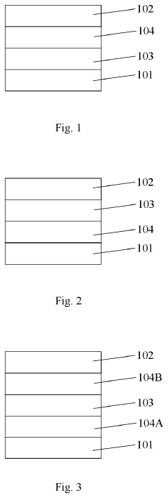
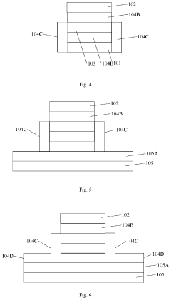
Resistive random access memory and manufacturing method thereof
PatentActiveUS20210028358A1
Innovation
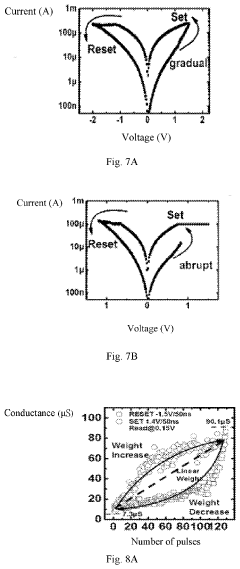
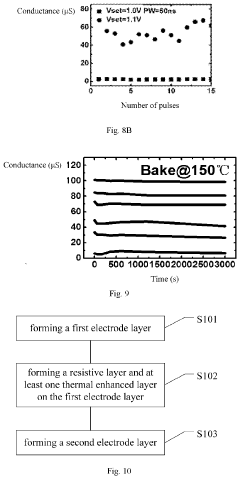
- Incorporating a thermal enhanced layer with lower thermal conductivity than the electrodes, positioned adjacent to the resistive layer, to slow down heat loss and promote the formation of dispersed conductive filaments, allowing continuous and bidirectional linear changes in conductance.
Resistive memory cell and operation thereof, and resistive memory and operation and fabrication thereof
PatentInactiveUS20120020140A1
Innovation
- The use of conductive domain walls in high-resistance ferroelectric materials, such as BiFeO3, to store data by applying voltage pulses and forming domains with varying polarities, allowing for efficient data storage with reduced power consumption.
Material Science Advancements for RRAM Optimization
Material science has emerged as a critical frontier in advancing RRAM (Resistive Random Access Memory) technology toward higher storage densities. Recent breakthroughs in switching materials have demonstrated significant improvements in memory cell reliability and endurance. Particularly, metal oxides such as HfOx, TaOx, and TiOx have shown promising characteristics with their controllable oxygen vacancy concentrations, which directly influence the formation and rupture of conductive filaments essential for RRAM operation.
The interface engineering between the switching layer and electrodes represents another crucial advancement area. Researchers have developed novel electrode materials and interface treatments that reduce variability in switching behavior while enhancing retention properties. For instance, the introduction of buffer layers between active materials and electrodes has demonstrated up to 40% improvement in switching uniformity across memory arrays.
Nanostructured materials have revolutionized RRAM design by enabling precise control over filament formation pathways. By incorporating engineered nanodots or nanolayers within the switching medium, researchers have achieved more predictable and controllable resistive switching. These nanostructures effectively constrain filament growth, resulting in more stable resistance states and lower operating voltages.
Composite materials combining multiple metal oxides or doped structures have shown exceptional promise for multi-level cell operations. These advanced material systems can maintain distinct resistance states with clearer separation margins, potentially increasing storage density by 2-4 times compared to binary storage approaches without increasing the physical footprint.
The development of two-dimensional materials for RRAM applications represents one of the most exciting frontiers. Materials such as graphene, MoS2, and h-BN have demonstrated unique switching characteristics when incorporated as either active layers or interface engineering elements. Their atomically thin nature enables extreme scaling potential while maintaining excellent electrical properties.
Temperature stability has been significantly enhanced through materials science innovations. New compositions with higher thermal conductivity and reduced thermal expansion coefficients maintain performance integrity across wider operating temperature ranges, addressing a critical limitation in previous RRAM generations. These thermally robust materials show less than 10% resistance drift across a 100°C operating range.
Looking forward, emerging research in self-healing materials may address endurance limitations in high-density RRAM. These materials can partially repair structural damage caused by repeated switching operations, potentially extending device lifetime by an order of magnitude and enabling more aggressive scaling for higher capacity storage solutions.
Energy Efficiency Considerations in High-Density RRAM
Energy efficiency has emerged as a critical factor in the development and deployment of high-density RRAM (Resistive Random Access Memory) technologies. As storage density increases, power consumption becomes a significant concern that can limit practical applications, particularly in mobile and IoT devices where battery life is paramount.
The fundamental energy requirements of RRAM operations stem from the SET and RESET processes that switch the resistance states of memory cells. Current high-density RRAM implementations typically consume between 0.1-10 pJ per bit operation, which represents a significant improvement over traditional flash memory but remains higher than theoretical limits. The energy consumption scales with array size, creating challenges for ultra-high-density implementations.
Voltage scaling techniques have shown promise in reducing energy consumption, with research demonstrating that operating voltages can be reduced to sub-1V levels while maintaining reliable switching behavior. This approach, however, often comes at the cost of increased switching time or reduced retention characteristics, necessitating careful optimization of the voltage-time-reliability relationship.
Material engineering presents another avenue for energy efficiency improvements. Alternative switching materials such as HfOx, TaOx, and various perovskite structures have demonstrated lower energy switching characteristics. Particularly promising are oxygen-engineered materials that facilitate more efficient filament formation and rupture processes, reducing the energy barrier for resistance switching.
Architectural innovations have also contributed significantly to energy efficiency. The crossbar architecture, while optimal for density, introduces sneak path currents that waste energy. Selector devices integrated with memory elements (1S1R configurations) effectively mitigate these parasitic currents, with recent selector technologies achieving high nonlinearity ratios (>10^4) while adding minimal energy overhead.
Advanced programming schemes represent another frontier in energy optimization. Adaptive programming algorithms that adjust pulse parameters based on cell characteristics have demonstrated energy reductions of up to 60% compared to fixed-parameter approaches. Multi-level cell (MLC) implementations, while increasing bit density, present additional energy challenges that require sophisticated programming algorithms to maintain efficiency.
Thermal management remains a critical consideration in high-density arrays, as localized heating during switching operations can affect neighboring cells and overall system reliability. Innovative heat dissipation structures and thermally optimized cell designs are being explored to address these challenges while maintaining the compact form factor necessary for high-density storage.
Unlock deeper insights with PatSnap Eureka Quick Research — get a full tech report to explore trends and direct your research. Try now!
Generate Your Research Report Instantly with AI Agent
Supercharge your innovation with PatSnap Eureka AI Agent Platform!