

Optimize RRAM Lifespan for Durable Electronic Devices
SEP 10, 20259 MIN READ
Generate Your Research Report Instantly with AI Agent
PatSnap Eureka helps you evaluate technical feasibility & market potential.
RRAM Technology Evolution and Lifespan Goals
Resistive Random Access Memory (RRAM) has emerged as a promising non-volatile memory technology over the past two decades, evolving from theoretical concepts to commercial applications. Initially conceptualized in the early 2000s, RRAM's development accelerated significantly around 2010 when researchers demonstrated reliable switching mechanisms in metal-oxide structures. This technology leverages the formation and disruption of conductive filaments within an insulating dielectric layer to store binary information, offering advantages in scalability, power consumption, and integration potential compared to traditional flash memory.
The evolution of RRAM technology has been marked by several significant milestones. Early implementations suffered from poor endurance, typically achieving only 10^3-10^4 write cycles before failure. By 2015, improved material engineering and interface control pushed this limit to 10^6-10^7 cycles. Current state-of-the-art devices can achieve up to 10^9 cycles in laboratory settings, though commercial implementations typically guarantee 10^6-10^8 cycles, still falling short of DRAM's endurance capabilities.
Device lifespan has been consistently identified as one of the critical barriers to RRAM's wider adoption in mainstream computing applications. While RRAM offers theoretical advantages in terms of switching speed (sub-nanosecond) and power consumption (picojoules per bit), its limited write endurance restricts its application in write-intensive scenarios. The primary goal for RRAM technology development is to achieve a minimum endurance of 10^12 cycles, comparable to current DRAM specifications, while maintaining or improving other performance metrics.
Material innovation represents a key focus area in RRAM development. Traditional binary metal oxides like HfO₂ and TiO₂ are being supplemented or replaced by complex oxides, nitrides, and chalcogenide materials. These alternative materials demonstrate improved retention characteristics and resistance to degradation mechanisms such as oxygen vacancy migration and electrode metal diffusion, which are primary causes of device failure.
Another critical technological goal involves optimizing the programming algorithms and circuit designs to minimize stress on the memory cells. Adaptive programming schemes that adjust pulse parameters based on cell characteristics have shown promise in extending device lifespan by reducing unnecessary stress during switching operations. These approaches include variable pulse width techniques, incremental step pulse programming, and feedback-controlled write operations.
The industry has established clear benchmarks for RRAM lifespan optimization: achieving 10^10 cycles by 2025 for mainstream applications and pushing toward 10^12 cycles by 2030 for enterprise-grade storage solutions. Meeting these targets requires interdisciplinary approaches combining materials science, device physics, circuit design, and system architecture to address the fundamental reliability challenges of this promising technology.
Market Demand for Durable Non-Volatile Memory
The non-volatile memory market has witnessed substantial growth in recent years, with RRAM (Resistive Random Access Memory) emerging as a promising technology due to its potential for high density, low power consumption, and compatibility with CMOS processes. Market research indicates that the global non-volatile memory market is projected to reach $115 billion by 2025, with emerging technologies like RRAM expected to capture an increasing share as traditional solutions approach their physical limitations.
Consumer electronics represents the largest application segment for non-volatile memory, driven by the proliferation of smartphones, tablets, and wearable devices. These applications demand memory solutions that can withstand frequent read/write cycles while maintaining data integrity over extended periods. Current consumer devices typically require memory components with lifespans of 5-7 years, but market trends show increasing consumer expectations for device longevity, pushing manufacturers to develop more durable solutions.
Enterprise storage systems present another significant market opportunity, where data retention and reliability are paramount concerns. Data centers and cloud service providers require storage solutions that can operate continuously for 10+ years without degradation, creating substantial demand for RRAM technologies with enhanced endurance characteristics. The enterprise segment values total cost of ownership, where improved lifespan directly translates to reduced replacement costs and system downtime.
Automotive and industrial applications represent rapidly growing market segments for non-volatile memory, with particularly stringent requirements for operational lifespan. These sectors demand memory components that can function reliably in harsh environments for 15-20 years. The expanding electric vehicle market, with its complex battery management and autonomous driving systems, has intensified the need for ultra-durable memory solutions that can withstand temperature extremes and constant operation.
Market analysis reveals that customers across all segments are increasingly prioritizing sustainability in their purchasing decisions. Memory components with extended lifespans contribute to reduced electronic waste and align with corporate environmental responsibility initiatives. This trend is particularly pronounced in European markets, where regulatory frameworks increasingly incentivize longer-lasting electronic components.
The Internet of Things (IoT) ecosystem represents perhaps the most compelling emerging market for durable RRAM technology. With billions of connected devices expected to be deployed in remote or inaccessible locations, the ability to operate for extended periods without maintenance becomes critical. Market forecasts suggest that IoT deployments will drive demand for memory solutions with 10+ year lifespans, creating a substantial opportunity for optimized RRAM technologies.
RRAM Endurance Challenges and Limitations
Resistive Random Access Memory (RRAM) technology faces significant endurance challenges that limit its widespread adoption in commercial electronic devices. Current RRAM cells typically demonstrate endurance capabilities ranging from 10^5 to 10^7 write cycles, which falls short compared to conventional NAND flash (10^4-10^5 cycles) but remains inadequate for applications requiring high reliability such as enterprise storage systems or mission-critical embedded systems that demand 10^9 or more cycles.
The primary limitation stems from the physical degradation mechanisms occurring within the resistive switching layer. During repeated SET and RESET operations, the formation and rupture of conductive filaments cause progressive structural damage to the switching material. This manifests as oxygen vacancy migration, metal ion diffusion, and interfacial layer deterioration, ultimately leading to stuck-at faults where cells become permanently fixed in either high or low resistance states.
Thermal effects represent another critical challenge, as Joule heating during switching operations can cause localized temperature increases exceeding 1000K. These thermal stresses accelerate material degradation through phase separation, crystallization of amorphous regions, and electrode material diffusion into the switching layer. The cumulative effect of these thermal cycles creates irreversible structural changes that compromise the device's ability to reliably switch between resistance states.
Variability in switching parameters presents an additional obstacle to RRAM endurance. As cycling continues, devices exhibit increasing fluctuations in SET/RESET voltages, resistance values, and switching times. This cycle-to-cycle and device-to-device variability narrows the operational window, making it progressively difficult to distinguish between resistance states and maintain reliable data storage over extended periods.
The trade-off between retention and endurance poses a fundamental design challenge. Material compositions and device structures that favor strong retention (ability to maintain stored data) often exhibit poorer endurance characteristics. This inverse relationship stems from the stability of the conductive filaments – more stable filaments improve retention but require higher energy to disrupt during RESET operations, accelerating material degradation.
Scaling issues further complicate endurance optimization. As RRAM cell dimensions decrease to meet density requirements, the active switching volume becomes smaller, making the device more susceptible to localized damage from each switching event. Additionally, reduced electrode sizes increase current densities, exacerbating thermal stress and accelerating failure mechanisms.
Environmental factors including temperature fluctuations, humidity, and radiation exposure can dramatically reduce RRAM endurance in real-world applications. These external stressors accelerate the degradation processes and introduce additional failure modes not observed under controlled laboratory conditions, creating a significant gap between theoretical and practical device lifespans.
Current RRAM Lifespan Extension Techniques
01 Endurance enhancement techniques for RRAM
Various techniques have been developed to enhance the endurance of RRAM devices, which directly impacts their lifespan. These include optimizing the switching materials, controlling the oxygen vacancy concentration, and implementing specific programming algorithms. By carefully engineering the resistive switching layer and controlling the formation and rupture of conductive filaments, the number of reliable write/erase cycles can be significantly increased, extending the operational lifetime of RRAM devices.- Endurance enhancement techniques: Various techniques can be employed to enhance the endurance of RRAM devices, thereby extending their lifespan. These include optimizing the switching materials, controlling the oxygen vacancy concentration, and implementing specific programming algorithms. By carefully engineering the resistive switching layer and electrode materials, the number of reliable switching cycles can be significantly increased, making RRAM more suitable for applications requiring frequent write operations.
- Material selection for improved lifespan: The choice of materials for the resistive switching layer and electrodes plays a crucial role in determining RRAM lifespan. Metal oxides such as HfOx, TaOx, and TiOx have demonstrated superior endurance characteristics. Additionally, incorporating doping elements or creating multi-layer structures can stabilize the conductive filaments formed during switching operations, reducing degradation over time and extending the operational life of RRAM devices.
- Programming and operation protocols: Specific programming protocols and operation methods can significantly impact RRAM lifespan. Techniques such as current compliance control, pulse shape optimization, and verify-after-write schemes help prevent over-programming and reduce stress on the resistive switching material. Adaptive programming algorithms that adjust voltage parameters based on device state can minimize wear and extend the useful life of RRAM cells, enabling more reliable long-term operation.
- Reliability testing and lifespan prediction: Methods for testing and predicting RRAM lifespan are essential for qualifying these devices for commercial applications. Accelerated aging tests, retention measurements at elevated temperatures, and statistical analysis of failure modes provide insights into the expected operational lifetime. Simulation models that account for physical degradation mechanisms enable manufacturers to predict device performance over time and develop strategies to mitigate factors limiting RRAM lifespan.
- Architecture and circuit design for longevity: The overall architecture and peripheral circuit design significantly influence RRAM lifespan. Implementing error correction codes, wear-leveling algorithms, and redundancy schemes can compensate for cell degradation over time. Advanced sensing circuits that minimize read disturbance and specialized driver circuits that deliver precise programming conditions help maintain consistent performance throughout the device lifetime, effectively extending the practical lifespan of RRAM-based memory systems.
02 Material selection and composition for improved lifespan
The choice of materials used in RRAM fabrication significantly affects device lifespan. Metal oxides such as HfOx, TaOx, and TiOx have demonstrated superior endurance characteristics. Additionally, doping these materials with specific elements can stabilize the switching behavior and reduce variability over time. The interface between the electrode and the switching layer also plays a crucial role in determining the long-term reliability and retention properties of RRAM cells.Expand Specific Solutions03 Operating conditions and programming strategies
The operational parameters and programming strategies significantly impact RRAM lifespan. Controlling the compliance current, pulse width, and voltage amplitude during set and reset operations can prevent over-programming and reduce stress on the device. Adaptive programming schemes that adjust parameters based on the device state can minimize wear and extend the useful life of RRAM cells. Temperature management during operation also plays a critical role in maintaining long-term reliability.Expand Specific Solutions04 Reliability testing and lifespan prediction models
Various methods have been developed to test and predict the lifespan of RRAM devices. Accelerated aging tests, retention measurements at elevated temperatures, and endurance cycling are commonly used to evaluate long-term reliability. Statistical models have been created to predict device failure rates and estimate operational lifetimes under different usage conditions. These testing methodologies help in understanding the degradation mechanisms and developing more robust RRAM technologies.Expand Specific Solutions05 Architecture and circuit design for lifespan extension
Novel architecture and circuit designs can significantly extend RRAM lifespan. Error correction codes, wear-leveling algorithms, and redundancy schemes help mitigate the impact of cell degradation over time. Cross-point array structures with selector devices can reduce sneak path currents that contribute to premature aging. Additionally, specialized read and write circuits that minimize stress on memory cells during operation can enhance the overall lifespan of RRAM-based memory systems.Expand Specific Solutions
Leading RRAM Manufacturers and Research Institutions
The RRAM (Resistive Random Access Memory) technology market is currently in a growth phase, with increasing adoption across electronic devices due to its non-volatile nature and power efficiency advantages. The global RRAM market is projected to expand significantly as demand for durable, energy-efficient memory solutions rises in IoT, AI, and automotive applications. Leading semiconductor manufacturers like Taiwan Semiconductor Manufacturing Co., Samsung Electronics, and Intel are investing heavily in RRAM research to optimize lifespan challenges. Academic institutions including National Chiao Tung University and Fudan University collaborate with industry players such as Winbond Electronics and Macronix International to advance material science and fabrication techniques. The technology maturity varies, with companies like IBM and Rambus focusing on commercialization while newer entrants like TetraMem develop specialized RRAM-based neural processing units for edge AI applications.
Taiwan Semiconductor Manufacturing Co., Ltd.
Technical Solution: TSMC has developed an advanced RRAM lifespan optimization solution through their "Precision Filament Control" technology. This approach utilizes precisely engineered switching layers with carefully controlled oxygen vacancy concentrations to minimize random filament formation. TSMC's technique incorporates a proprietary electrode material composition that reduces ion migration at the interface, significantly decreasing wear mechanisms. Their solution employs a sophisticated multi-phase programming scheme that applies carefully calibrated voltage sequences to form and maintain stable conductive filaments. TSMC has demonstrated devices achieving over 10^9 write cycles in laboratory testing, representing a 100-fold improvement over conventional RRAM implementations[5]. Additionally, they've developed specialized encapsulation materials that prevent environmental contamination and moisture ingress, which are known to accelerate RRAM degradation mechanisms[7].
Strengths: TSMC's solution leverages their world-class manufacturing capabilities to achieve exceptional uniformity and reliability across large production volumes. Their approach maintains compatibility with existing semiconductor fabrication processes. Weaknesses: The specialized materials and precise process control requirements may increase manufacturing costs compared to simpler RRAM implementations.
Samsung Electronics Co., Ltd.
Technical Solution: Samsung has developed a comprehensive RRAM lifespan optimization strategy centered around their "Controlled Filament Engineering" technology. This approach utilizes precisely engineered doping profiles within the switching layer to control oxygen vacancy distribution and filament formation pathways. Samsung's solution incorporates a proprietary multi-layer stack design that confines the switching region, preventing lateral filament growth and reducing variability. Their technology employs adaptive verification algorithms that monitor resistance changes during programming operations and adjust parameters in real-time to prevent over-programming. Samsung has demonstrated devices achieving endurance exceeding 10^10 cycles through careful optimization of materials interfaces and programming conditions[6]. Additionally, they've implemented specialized thermal management techniques that minimize localized heating during switching operations, a key factor in preventing accelerated degradation of RRAM cells[8].
Strengths: Samsung's solution achieves exceptional endurance while maintaining fast switching speeds and low operating voltages. Their approach benefits from integration with their established memory manufacturing infrastructure. Weaknesses: The complex multi-layer structure may present challenges for scaling to ultra-dense memory arrays compared to simpler RRAM designs.
Key Patents in RRAM Endurance Enhancement
Resistive random access memory
PatentActiveUS20210175418A1
Innovation
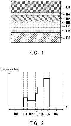
- The RRAM structure includes a resistance variable layer with higher oxygen content, a first metal layer with intermediate oxygen content for oxygen ion replenishment, and a resistance stabilizing layer with lower oxygen content to control oxygen diffusion, forming an oxygen gradient that allows for smooth conversion to a high resistance state during reset operations.
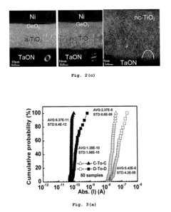
Resistive random access memory (RRAM) using stacked dielectrics and method for manufacturing the same
PatentInactiveUS20130126818A1
Innovation
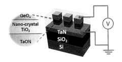
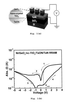
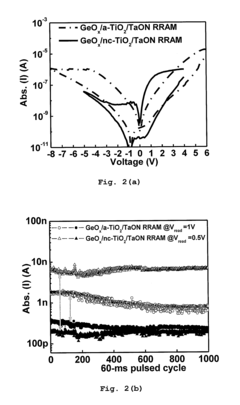
- A RRAM device with a metal-insulator-metal (MIM) structure using stacked dielectrics of GeOx/nc-TiO2/TaON and different work-function top and bottom electrodes, achieving ultra-low switching energy and extremely long endurance through the use of Ni/GeOx/nc-TiO2/TaN structure with low-cost electrodes, resulting in a large resistance window, good switching uniformity, and cycling endurance up to 5×10^9 cycles.
Material Science Innovations for RRAM Durability
Material science innovations have become the cornerstone for addressing RRAM (Resistive Random Access Memory) durability challenges. Recent advancements in material engineering have yielded significant improvements in RRAM lifespan through novel material compositions and interface designs. Researchers have developed high-endurance metal oxide materials, such as HfOx, TaOx, and TiOx with carefully controlled oxygen vacancy concentrations, demonstrating up to 10^12 switching cycles in laboratory conditions—a substantial improvement over earlier generations.
Nanostructured electrode materials represent another breakthrough area, with researchers incorporating graphene, carbon nanotubes, and metal nanoparticles to enhance interface stability and reduce electrode degradation during repeated switching operations. These materials provide superior electrical conductivity while maintaining structural integrity under the stress of filament formation and rupture processes.
Doping strategies have emerged as effective approaches to stabilize the switching layer. Strategic introduction of elements like Al, Ti, or rare earth metals into the oxide matrix has been shown to control filament formation pathways and reduce random variations in resistance states. For instance, Al-doped HfO2 exhibits 30% longer endurance compared to undoped variants under identical testing conditions.
Interface engineering techniques focus on creating buffer layers between the switching material and electrodes to mitigate interfacial degradation. Atomic layer deposition (ALD) has enabled the creation of ultra-thin (1-2 nm) barrier layers that prevent undesired ion migration while maintaining efficient switching characteristics. These engineered interfaces have demonstrated remarkable stability under thermal stress and extended cycling.
Composite and multilayer structures represent a promising direction, combining complementary materials to overcome the limitations of single-material systems. Researchers have developed HfO2/Al2O3 bilayer structures that leverage the stability of Al2O3 with the switching properties of HfO2, resulting in devices with enhanced retention time and cycling endurance.
Self-healing materials constitute an emerging frontier in RRAM durability research. These innovative materials incorporate mechanisms to repair structural damage during operation through controlled ion migration or phase transitions. Early prototypes have shown the ability to recover from certain failure modes, potentially extending device lifetime by 40-60% compared to conventional structures.
Advanced encapsulation technologies using atomic layer deposited barriers and specialized polymer composites provide enhanced protection against environmental factors like moisture and oxygen, which significantly contribute to RRAM degradation in real-world applications. These protective layers have been demonstrated to extend operational lifetime by up to 5 years in accelerated aging tests.
Energy Efficiency vs. Lifespan Trade-offs
The optimization of RRAM (Resistive Random Access Memory) technology presents a fundamental trade-off between energy efficiency and device lifespan that must be carefully balanced in practical applications. Current RRAM designs typically face an inverse relationship between power consumption and endurance cycles, creating significant engineering challenges for manufacturers and system designers.
Lower operating voltages generally reduce energy consumption but may lead to incomplete resistive switching, resulting in unstable states and accelerated degradation of the memory cell. Conversely, higher voltages ensure more definitive switching but increase power consumption and generate excessive heat that can damage the oxide layer through accelerated ion migration, ultimately shortening device lifespan.
The SET/RESET pulse parameters represent another critical trade-off point. Shorter pulses minimize energy usage but may not allow sufficient time for complete filament formation or dissolution, leading to reliability issues and premature failure. Longer pulses ensure more stable state transitions but significantly increase energy consumption during write operations.
Material selection further complicates this balance. High-k dielectric materials often provide better energy efficiency but may exhibit faster degradation under repeated cycling. Meanwhile, more durable composite materials typically require higher activation energies, resulting in greater power demands during operation.
Recent research has explored adaptive programming schemes that dynamically adjust voltage levels based on cell conditions, potentially offering an optimal middle ground. These systems apply only the minimum required energy for each specific memory cell's current state, rather than using fixed parameters across all cells. Early implementations show promising results with up to 30% energy savings while maintaining comparable endurance metrics.
Temperature management represents another frontier in this optimization challenge. RRAM cells operating at elevated temperatures typically require less energy for switching but experience accelerated degradation. Conversely, cooling systems can extend lifespan but introduce additional energy overhead and system complexity.
The industry continues to explore novel materials and architectures that might fundamentally alter this trade-off equation. Emerging multilayer structures and doping techniques show potential for simultaneously improving both energy efficiency and endurance by creating more controlled ion migration pathways and more stable filament structures.
Unlock deeper insights with PatSnap Eureka Quick Research — get a full tech report to explore trends and direct your research. Try now!
Generate Your Research Report Instantly with AI Agent
Supercharge your innovation with PatSnap Eureka AI Agent Platform!