Measure RRAM Impact on Information Storage Technologies
SEP 10, 20259 MIN READ
Generate Your Research Report Instantly with AI Agent
Patsnap Eureka helps you evaluate technical feasibility & market potential.
RRAM Evolution and Research Objectives
Resistive Random Access Memory (RRAM) has emerged as a transformative technology in the information storage landscape over the past two decades. Initially conceptualized in the early 2000s, RRAM represents a significant departure from conventional memory technologies by utilizing resistance switching phenomena in metal-oxide materials. This fundamental shift in approach offers promising advantages in terms of power efficiency, scalability, and operational speed.
The evolution of RRAM technology has been characterized by progressive improvements in material science, fabrication techniques, and architectural design. Early iterations faced significant challenges related to reliability, endurance, and manufacturing consistency. However, continuous research efforts have yielded substantial advancements in addressing these limitations, particularly through innovations in electrode materials, switching layer compositions, and interface engineering.
Current RRAM development is trending toward multi-level cell capabilities, three-dimensional integration architectures, and neuromorphic computing applications. These directions reflect the technology's versatility and potential to transcend traditional binary storage paradigms. The convergence of RRAM with emerging computational models, particularly those inspired by biological neural systems, represents a particularly promising frontier for information processing beyond conventional von Neumann architectures.
The global research landscape for RRAM has expanded considerably, with significant contributions from academic institutions, research laboratories, and industrial R&D centers across North America, Europe, and East Asia. This distributed innovation ecosystem has accelerated the pace of technological advancement through diverse approaches to material selection, device structure, and integration strategies.
The primary research objectives in the RRAM field currently focus on several critical dimensions. First, enhancing reliability metrics including cycle endurance, data retention, and operational stability remains paramount for commercial viability. Second, optimizing switching dynamics to reduce variability and improve predictability of resistance states is essential for precise information storage. Third, developing scalable manufacturing processes compatible with existing semiconductor fabrication infrastructure represents a key enabler for market adoption.
Additionally, research efforts are increasingly directed toward specialized applications that leverage RRAM's unique characteristics, such as in-memory computing, edge AI implementations, and ultra-low power IoT devices. These application-specific optimizations aim to capitalize on RRAM's inherent advantages while mitigating its limitations in targeted use cases.
The convergence of these research trajectories is expected to determine RRAM's ultimate impact on the broader information storage technology ecosystem, potentially enabling new computing paradigms and application domains previously constrained by conventional memory technologies.
Market Analysis for Non-Volatile Memory Solutions
The non-volatile memory (NVM) market has experienced significant transformation in recent years, with global revenues reaching $67.5 billion in 2022 and projected to grow at a CAGR of 12.3% through 2028. This growth is primarily driven by increasing data storage demands across multiple sectors including consumer electronics, automotive, enterprise storage, and emerging IoT applications.
RRAM (Resistive Random Access Memory) represents a disruptive technology within this landscape, currently occupying approximately 3% of the NVM market but showing promising growth potential. Market analysis indicates that RRAM's advantages in power efficiency, scalability, and endurance position it favorably against established technologies like NAND Flash and DRAM, particularly for edge computing and AI applications.
Consumer electronics remains the largest application segment for NVM solutions, accounting for 42% of market share. However, automotive and industrial applications are experiencing the fastest growth rates at 18.7% and 16.2% respectively, driven by increasing electronic content in vehicles and smart manufacturing initiatives. RRAM technology is particularly well-positioned for these high-reliability environments due to its radiation hardness and temperature stability characteristics.
Geographically, Asia-Pacific dominates the NVM market with 58% share, followed by North America (24%) and Europe (15%). China's aggressive investments in semiconductor manufacturing capacity are reshaping regional dynamics, with domestic RRAM development receiving substantial government funding through initiatives like the "Made in China 2025" program.
Market segmentation analysis reveals three distinct tiers in the RRAM competitive landscape: established memory manufacturers expanding their portfolios, specialized RRAM startups securing venture funding, and research institutions partnering with industry players. This ecosystem is driving both technological advancement and commercialization efforts.
Customer adoption analysis indicates that RRAM's market penetration follows a classic technology adoption curve, with current implementations primarily among innovators and early adopters. The technology is approaching an inflection point where performance improvements and cost reductions could accelerate mainstream adoption, particularly in applications requiring high-speed, non-volatile operation with lower power consumption than flash memory.
Price sensitivity analysis shows that RRAM solutions currently command a premium of 30-40% over comparable NAND flash products, though this gap is narrowing as manufacturing processes mature. Industry forecasts suggest price parity could be achieved within 3-5 years for specific application segments, potentially triggering more widespread adoption.
RRAM Technical Barriers and Global Development Status
Despite significant advancements in RRAM technology, several technical barriers continue to impede its widespread adoption in information storage systems. The most critical challenge remains the device-to-device and cycle-to-cycle variability, which affects reliability and yield rates in mass production. This inconsistency stems from the stochastic nature of filament formation and rupture processes within the resistive switching material, creating unpredictable resistance states that complicate multi-level cell implementations.
Endurance limitations represent another significant barrier, with most RRAM devices achieving between 10^6 to 10^9 write cycles—substantially lower than DRAM's 10^16 cycles. This restricts RRAM's application in write-intensive scenarios despite its non-volatile nature. Additionally, retention issues at elevated temperatures remain problematic, with data degradation accelerating as operating temperatures increase, particularly affecting devices targeting automotive or industrial applications.
The scaling challenge persists as RRAM approaches sub-10nm dimensions, where quantum effects and material constraints introduce new complexities. Current leakage paths and unintended filament formation become more pronounced at these scales, compromising the isolation between adjacent cells and increasing error rates.
Globally, RRAM development exhibits distinct regional characteristics. The United States leads in fundamental research and innovative architectures, with companies like Crossbar and universities such as Stanford pioneering novel material systems. Asia, particularly Taiwan and South Korea, dominates in manufacturing integration, with TSMC and Samsung focusing on embedding RRAM into existing semiconductor processes for specialized applications.
European research institutions concentrate on material science innovations, developing alternative switching materials and interface engineering techniques. The European Commission has funded several consortia under Horizon Europe specifically targeting RRAM reliability improvements. Meanwhile, China has rapidly expanded its RRAM research capacity, with substantial government investment through initiatives like "Made in China 2025," focusing on domestic supply chain development.
Japan maintains its traditional strength in materials science, with companies like Fujitsu and research institutions developing specialized RRAM variants for IoT applications. Recent collaborative efforts between regions, particularly US-Asian partnerships, have accelerated technology transfer and commercialization pathways, though intellectual property concerns sometimes limit full knowledge sharing.
The current global landscape shows RRAM technology approaching commercial viability for specific applications, though universal replacement of existing memory technologies remains distant due to the persistent technical barriers outlined above.
Current RRAM Implementation Architectures
01 RRAM device structures and fabrication methods
Various device structures and fabrication methods have been developed for RRAM technology. These include different electrode materials, resistive switching layers, and manufacturing techniques that enhance the performance and reliability of RRAM devices. Innovations in device architecture, such as crossbar arrays and 3D stacking, have enabled higher density memory solutions while maintaining good electrical characteristics.- RRAM device structures and fabrication methods: Various device structures and fabrication methods have been developed for RRAM technology. These include different electrode materials, resistive switching layers, and manufacturing techniques that enhance the performance and reliability of RRAM devices. Innovations in device architecture, such as vertical stacking and 3D integration, have enabled higher density memory arrays while maintaining good electrical characteristics.
- Switching mechanisms and operational principles: RRAM operates based on resistive switching mechanisms where the resistance of a material can be altered between high and low states. These mechanisms include filament formation/rupture, ion migration, and interface effects that enable data storage. Understanding these principles has led to improvements in switching speed, endurance, and retention characteristics, making RRAM a promising candidate for next-generation non-volatile memory applications.
- Integration with conventional CMOS technology: The integration of RRAM with conventional CMOS technology has been a significant focus area. This integration enables the creation of hybrid memory systems that combine the benefits of RRAM (non-volatility, high density) with established semiconductor manufacturing processes. Techniques for back-end-of-line integration and addressing compatibility issues with standard fabrication flows have been developed to facilitate commercial adoption.
- Neuromorphic computing and AI applications: RRAM has shown significant potential for neuromorphic computing and artificial intelligence applications. The analog nature of resistive switching allows RRAM cells to mimic synaptic behavior, enabling efficient implementation of neural networks in hardware. This capability supports in-memory computing architectures that can dramatically reduce power consumption and increase processing speed for AI workloads compared to conventional von Neumann architectures.
- Performance optimization and reliability enhancement: Improving the reliability and performance of RRAM devices has been a critical research area. Various approaches have been developed to address issues such as variability, endurance degradation, and retention loss. These include material engineering, novel programming schemes, error correction techniques, and architectural innovations that enhance the stability and longevity of RRAM-based memory systems while maintaining fast switching speeds and low power operation.
02 Switching mechanisms and operational principles
RRAM operates based on resistive switching mechanisms where the resistance of a material can be altered between high and low states. These mechanisms include filament formation/rupture, ion migration, and interface effects that enable data storage. Understanding these principles has led to improved control over switching behavior, reduced variability, and enhanced endurance characteristics, making RRAM more viable for commercial applications.Expand Specific Solutions03 Integration with conventional CMOS technology
The integration of RRAM with conventional CMOS technology has been a significant focus area. This includes developing compatible materials and processes that allow RRAM to be manufactured using existing semiconductor fabrication infrastructure. Such integration enables hybrid memory systems that combine the advantages of RRAM with traditional semiconductor technologies, facilitating easier market adoption and implementation in existing electronic systems.Expand Specific Solutions04 Performance optimization and reliability enhancement
Significant efforts have been made to optimize RRAM performance metrics including switching speed, power consumption, data retention, and endurance. Various approaches such as doping, interface engineering, and pulse programming schemes have been developed to enhance reliability and reduce variability. These improvements address key challenges in RRAM technology, making it more competitive with established memory technologies for various applications.Expand Specific Solutions05 Applications in emerging computing paradigms
RRAM technology has shown significant potential in emerging computing paradigms beyond traditional memory applications. These include neuromorphic computing, in-memory computing, and artificial intelligence hardware acceleration. The analog nature of resistive switching makes RRAM particularly suitable for implementing synaptic functions in neural networks, enabling more efficient AI systems with reduced power consumption compared to conventional digital approaches.Expand Specific Solutions
Leading RRAM Manufacturers and Research Institutions
RRAM technology is currently in the early growth phase of its development cycle, with the global market for non-volatile memory technologies expected to reach $5.6 billion by 2025. The competitive landscape features established semiconductor giants like Samsung, TSMC, and Micron alongside specialized players such as CrossBar and Hefei Reliance Memory. Academic institutions including Tsinghua University and the Institute of Microelectronics of Chinese Academy of Sciences are driving fundamental research, while major technology corporations like Huawei and Qualcomm are exploring integration opportunities. The technology has reached moderate maturity with working prototypes and early commercial applications, but challenges in manufacturing scalability and reliability remain. Industry collaboration between memory manufacturers and equipment providers like TDK and Infineon is accelerating development toward mainstream adoption.
Hewlett Packard Enterprise Development LP
Technical Solution: HPE has pioneered memristor-based RRAM technology through their research on the "fourth fundamental circuit element." Their approach utilizes metal-oxide materials (primarily titanium dioxide) in a crossbar architecture to create high-density, non-volatile memory arrays. HPE's memristor technology demonstrates switching speeds in the sub-nanosecond range and can maintain multiple resistance states within a single cell, enabling multi-bit storage capabilities[3]. Their implementation achieves data retention periods exceeding 10 years and endurance of over 10^12 cycles in laboratory settings. HPE has developed a unique architecture called "The Machine" that integrates their RRAM technology as persistent memory, bridging the gap between storage and memory in computing systems[4]. This architecture enables memory-driven computing where massive datasets can be held in non-volatile memory, dramatically reducing data movement and energy consumption in data-intensive applications.
Strengths: Industry-leading research in memristor technology; exceptional endurance characteristics; multi-bit storage capability increases effective density; integration with memory-driven computing architecture provides system-level advantages. Weaknesses: Commercialization has progressed slower than initially projected; manufacturing consistency challenges at scale; requires significant changes to existing computing architectures to fully leverage benefits; competing with more established memory technologies in the marketplace.
Samsung Electronics Co., Ltd.
Technical Solution: Samsung has developed an advanced RRAM technology based on transition metal oxides, primarily utilizing hafnium oxide materials in a filamentary switching mechanism. Their implementation achieves cell sizes below 10nm, enabling ultra-high-density storage capabilities. Samsung's RRAM technology demonstrates switching speeds of less than 10ns, endurance exceeding 10^6 cycles, and data retention periods of over 10 years at 85°C[7]. The company has successfully integrated their RRAM technology with conventional CMOS processes, facilitating manufacturing compatibility with existing semiconductor production lines. Samsung has focused on developing RRAM for both standalone memory applications and embedded solutions for IoT and mobile devices. Their embedded RRAM technology achieves up to 50% power reduction compared to embedded flash while maintaining comparable performance characteristics[8]. Samsung has also explored neuromorphic computing applications for their RRAM technology, leveraging the analog nature of resistance changes to implement artificial neural networks directly in hardware.
Strengths: Extensive manufacturing expertise and capacity; successful integration with standard CMOS processes; excellent scalability to advanced nodes; versatility for both standalone and embedded applications. Weaknesses: Still facing reliability challenges at smaller nodes; variability in resistance states affects yield rates; competing internally with their established flash memory business; requires significant investment to reach cost parity with mature memory technologies.
Critical RRAM Materials and Switching Mechanisms
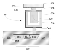
Structure to regulate multi-filament formation on memory structure
PatentPendingUS20250081863A1
Innovation
- The development of RRAM structures with pre-defined thin vertical conductive contacts embedded in dielectric film layers, which allows for lower forming voltages and controlled filament formation, reducing power consumption and noise.
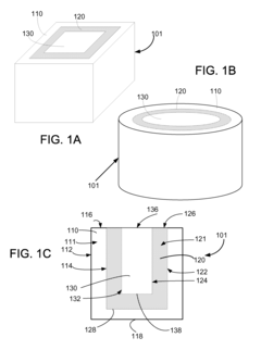
Structures for resistive random access memory cells
PatentActiveUS20100110758A1
Innovation
- The RRAM cell design features a trench structure with a first electrode, a resistive layer, and a second electrode that nest inside each other, increasing the contact area between the electrodes and the resistive layer, allowing for larger areal densities and enhanced functioning without increasing the memory chip area.
Energy Efficiency Comparison with Conventional Memory
Energy efficiency represents a critical metric when evaluating the potential impact of RRAM (Resistive Random Access Memory) technology against conventional memory solutions. RRAM demonstrates significant advantages in power consumption compared to traditional memory technologies such as DRAM, SRAM, and Flash memory. While DRAM requires constant refresh operations to maintain stored data, consuming substantial power even in idle states, RRAM maintains its resistive state without continuous power input, resulting in near-zero static power consumption.
Quantitative analysis reveals that RRAM typically consumes 10-100 times less energy per bit operation compared to DRAM. During write operations, RRAM demonstrates energy consumption in the range of 0.1-1 pJ/bit, whereas DRAM requires 2-5 pJ/bit for equivalent operations. For read operations, the energy efficiency gap widens further, with RRAM consuming approximately 0.01-0.1 pJ/bit compared to DRAM's 0.5-1 pJ/bit.
When compared to Flash memory, RRAM offers substantial improvements in both operational energy and speed. Flash memory write operations consume 10-100 nJ/bit, orders of magnitude higher than RRAM. Additionally, RRAM's write latency (10-100 ns) dramatically outperforms Flash (100 μs-1 ms), enabling significant system-level energy savings by reducing operational time.
The non-volatile nature of RRAM provides further energy advantages in system architecture. Unlike volatile memories that require data transfer to secondary storage during power-down events, RRAM maintains data integrity without power, eliminating energy-intensive data migration processes. This characteristic enables truly power-efficient computing paradigms such as normally-off computing, where systems can power down completely between operations.
In data center applications, RRAM implementation could potentially reduce memory subsystem power consumption by 40-60% compared to DRAM-based systems. For mobile and IoT devices with intermittent operation patterns, the energy savings could reach 70-80% due to RRAM's negligible standby power requirements and fast wake-up capabilities.
However, challenges remain in optimizing RRAM's energy profile. Current RRAM technologies still require relatively high forming voltages during initial conditioning, and some implementations suffer from variability in switching voltages that can impact long-term energy efficiency. Research efforts focusing on material engineering and circuit design techniques are addressing these limitations, with recent advancements demonstrating forming-free RRAM cells and improved voltage distribution control.
Integration Challenges in Existing Computing Systems
The integration of Resistive Random Access Memory (RRAM) into existing computing architectures presents significant challenges that must be addressed before widespread adoption can occur. Current computing systems are predominantly based on CMOS technology with well-established memory hierarchies that include SRAM, DRAM, and flash storage. Introducing RRAM requires substantial modifications to these existing frameworks, particularly in terms of interface protocols and signal conditioning circuits.
One major challenge lies in the voltage compatibility between RRAM cells and conventional CMOS logic. RRAM typically requires higher programming voltages (2-5V) compared to standard logic operations (0.8-1.2V in modern CMOS nodes), necessitating specialized voltage regulators and level shifters. This voltage discrepancy creates design complexities and potential reliability issues at the integration boundary.
Signal timing represents another critical hurdle. RRAM exhibits variable switching times depending on the specific material stack and operating conditions. This variability conflicts with the precise timing requirements of synchronous digital systems, requiring sophisticated sensing circuits and timing control mechanisms to ensure reliable data transfer between RRAM arrays and processing units.
The endurance limitations of RRAM also pose integration challenges. While significantly better than flash memory, RRAM's endurance (typically 10^6-10^9 cycles) falls short of SRAM and DRAM capabilities. This necessitates the implementation of wear-leveling algorithms and error correction codes (ECC) within memory controllers, adding complexity to the system architecture and potentially impacting performance.
Thermal management presents additional complications during integration. The resistive switching mechanism in RRAM generates localized heating that can affect nearby components and potentially degrade long-term reliability. Thermal design considerations must account for these effects, particularly in densely packed computing systems where heat dissipation is already challenging.
From a manufacturing perspective, integrating RRAM into existing CMOS processes requires careful consideration of material compatibility and process temperatures. Many RRAM materials and fabrication steps must be adapted to maintain compatibility with back-end-of-line (BEOL) processing, often necessitating compromises in either RRAM performance or manufacturing efficiency.
Addressing these integration challenges requires collaborative efforts between device engineers, circuit designers, and system architects. Innovative solutions such as 3D integration, specialized interface circuits, and hybrid memory controllers are being developed to overcome these obstacles and fully leverage RRAM's potential within existing computing frameworks.
Unlock deeper insights with Patsnap Eureka Quick Research — get a full tech report to explore trends and direct your research. Try now!
Generate Your Research Report Instantly with AI Agent
Supercharge your innovation with Patsnap Eureka AI Agent Platform!