

Quantifying RRAM Capacities in Large Data Arrays
SEP 10, 20259 MIN READ
Generate Your Research Report Instantly with AI Agent
Patsnap Eureka helps you evaluate technical feasibility & market potential.
RRAM Technology Evolution and Objectives
Resistive Random-Access Memory (RRAM) has emerged as a promising non-volatile memory technology over the past two decades, evolving from theoretical concepts to practical implementations. The evolution of RRAM technology began in the early 2000s with the discovery of resistive switching phenomena in various metal oxide materials. Initial research focused on understanding the fundamental mechanisms of resistive switching, which involves the formation and rupture of conductive filaments within an insulating layer.
By the mid-2000s, researchers had demonstrated basic RRAM cells with binary storage capabilities, marking the first generation of RRAM devices. These early implementations suffered from reliability issues, including limited endurance and retention. The second generation, emerging around 2010, addressed these challenges through improved material engineering and device architectures, enabling more stable switching behavior and longer retention times.
The current third generation of RRAM technology has shifted focus toward multi-level cell capabilities and integration into large arrays, which is crucial for high-density storage applications. This evolution has been driven by the increasing demand for storage solutions that combine the speed of DRAM with the non-volatility of flash memory, while offering higher density and lower power consumption.
A significant technological milestone was reached when researchers demonstrated that RRAM could achieve switching speeds in the nanosecond range, comparable to DRAM but with non-volatile characteristics. This breakthrough opened possibilities for RRAM as a universal memory solution that could potentially replace both DRAM and flash in certain applications.
The primary objective in quantifying RRAM capacities in large data arrays is to establish reliable metrics for evaluating the practical storage density and performance of RRAM-based memory systems. This involves developing methodologies to accurately measure and predict the effective bit capacity of RRAM arrays under various operating conditions, considering factors such as cell-to-cell variability, noise margins, and error rates.
Another critical objective is to understand the scaling limitations of RRAM technology in large arrays. As cell sizes decrease and array sizes increase, new challenges emerge related to sneak path currents, voltage distribution, and thermal effects that can impact the reliable operation of the memory array. Quantifying these effects is essential for developing effective mitigation strategies.
The long-term technological goal is to enable RRAM as a viable solution for high-density storage in data-intensive applications, including artificial intelligence, edge computing, and the Internet of Things. This requires not only improving the fundamental cell characteristics but also developing sophisticated array architectures and control schemes that maximize the effective storage capacity while maintaining reliability and performance.
Market Analysis for RRAM Data Storage Solutions
The RRAM (Resistive Random Access Memory) data storage market is experiencing significant growth as organizations seek more efficient solutions for handling large data arrays. Current market analysis indicates that the global RRAM market is projected to reach $4.6 billion by 2027, growing at a compound annual growth rate of 16.2% from 2022. This growth is primarily driven by increasing demand for high-density, non-volatile memory solutions that can address the limitations of conventional storage technologies.
The enterprise sector represents the largest market segment for RRAM solutions, accounting for approximately 42% of the total market share. This is attributed to the escalating need for faster data processing capabilities and reduced power consumption in data centers. Cloud service providers are increasingly adopting RRAM technologies to enhance their storage infrastructure performance, with major players like Amazon Web Services and Microsoft Azure conducting extensive testing of RRAM-based storage systems.
Consumer electronics follows as the second-largest market segment, representing about 31% of the market. The integration of RRAM in smartphones, tablets, and wearable devices is gaining momentum due to its superior performance characteristics, including faster read/write speeds and lower power requirements compared to traditional flash memory.
Geographically, North America leads the RRAM market with approximately 38% market share, followed by Asia-Pacific at 34%. The Asia-Pacific region, however, is expected to witness the highest growth rate of 18.7% during the forecast period, primarily due to the strong presence of semiconductor manufacturers and increasing investments in memory technologies in countries like South Korea, Japan, and China.
Market analysis reveals that the capacity to quantify and optimize RRAM performance in large data arrays is becoming a critical differentiator for vendors. Organizations are increasingly seeking solutions that can provide precise metrics on storage density, endurance cycles, and power efficiency. This trend is particularly evident in the financial services and healthcare sectors, where the ability to process vast amounts of data quickly and efficiently is paramount.
The competitive landscape is characterized by both established semiconductor companies and innovative startups. Industry leaders like Samsung Electronics, Intel, and Micron Technology are investing heavily in RRAM research and development, while startups such as Crossbar and Weebit Nano are focusing on specialized RRAM solutions for specific market applications.
Customer demand patterns indicate a growing preference for integrated RRAM solutions that offer seamless compatibility with existing storage infrastructures while providing clear performance advantages. The market is also witnessing increased interest in hybrid storage systems that combine RRAM with other memory technologies to optimize performance across different workload types.
Current RRAM Capacity Limitations and Challenges
Despite significant advancements in Resistive Random Access Memory (RRAM) technology, several critical limitations persist when implementing large-scale data arrays. The primary challenge remains the device-to-device and cycle-to-cycle variability, which becomes increasingly problematic as array sizes scale up. This variability manifests as inconsistent resistance states across different cells, leading to potential data corruption and reliability issues in large arrays. Statistical analysis reveals that this variability can cause up to 15-20% deviation in resistance values, significantly impacting the overall storage capacity and reliability.
Another fundamental limitation is the sneak path current problem inherent to crossbar architectures. As array dimensions increase, parasitic current paths through neighboring cells create read disturbances and power inefficiencies. Current mitigation strategies such as selector devices add complexity and manufacturing challenges, ultimately constraining practical array sizes to approximately 1Mb per layer without significant performance compromises.
Endurance limitations present another significant barrier to large-scale RRAM implementation. While single RRAM cells have demonstrated endurance of 10^6-10^9 cycles in laboratory settings, this performance degrades substantially in large arrays due to cumulative stress effects and non-uniform wear patterns. Recent studies indicate that in arrays exceeding 256×256 cells, average endurance can drop by an order of magnitude, severely limiting applications requiring frequent write operations.
The retention characteristics of RRAM cells also pose challenges for large arrays. Data retention typically ranges from 10 years at room temperature to mere months at elevated temperatures (85°C+). This temperature sensitivity becomes more pronounced in dense arrays where thermal management is complicated by proximity effects. Quantitative models suggest that retention failures increase exponentially with array size due to the statistical nature of retention failure mechanisms.
Energy consumption scales non-linearly with array size, presenting another limitation. While individual RRAM cells offer low-power operation (typically 0.1-10 pJ per operation), the cumulative effect in large arrays, combined with peripheral circuitry overhead, results in significant power requirements. Recent benchmarking studies demonstrate that power efficiency decreases by approximately 30% when scaling from small (64×64) to large (1024×1024) arrays.
Finally, the read/write speed disparity becomes more pronounced in large arrays. While single-cell operations can achieve sub-nanosecond switching, practical large array implementations typically operate at microsecond timescales due to parasitic capacitances, resistance-capacitance delays, and peripheral circuit limitations. This speed limitation directly impacts the maximum achievable bandwidth, creating a fundamental capacity-performance tradeoff in large-scale RRAM implementations.
Methodologies for RRAM Capacity Quantification
01 High-density RRAM architectures
Advanced architectures for RRAM that enable high-density memory storage capabilities. These designs include 3D stacking, crossbar arrays, and multi-level cell configurations that significantly increase storage capacity while maintaining a small physical footprint. These architectures allow for terabit-scale storage in RRAM devices, making them competitive with traditional storage technologies while offering the benefits of non-volatility and lower power consumption.- RRAM device structures and fabrication methods: Various device structures and fabrication methods are employed to enhance RRAM capacities. These include multi-layer stacking techniques, novel electrode materials, and specialized deposition processes that improve memory density. Advanced manufacturing approaches enable the creation of high-capacity RRAM cells with optimized switching layers and interfaces, contributing to increased storage density and improved performance characteristics.
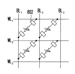
- Memory cell array architectures for high-capacity RRAM: Innovative memory cell array architectures are designed to maximize RRAM storage capacity. These architectures include crossbar arrays, 3D vertical stacking, and high-density integration schemes that optimize the spatial arrangement of memory cells. Such configurations allow for greater bit density per unit area, enabling higher overall memory capacity while maintaining reliable operation and addressing capabilities.
- Switching mechanisms and materials for enhanced storage density: Research into switching mechanisms and materials focuses on improving RRAM storage density. Various resistive switching materials, including metal oxides and novel compounds, are investigated to achieve multiple resistance states within a single memory cell. Multi-level cell (MLC) and multi-bit storage approaches enable storing more than one bit of information per cell, significantly increasing the effective capacity of RRAM devices.
- Control and sensing circuits for high-capacity operation: Specialized control and sensing circuits are developed to support high-capacity RRAM operation. These circuits include advanced read/write schemes, precise current control mechanisms, and noise-resistant sensing techniques that enable reliable operation at higher densities. Circuit innovations help overcome challenges related to sneak paths, read disturbance, and variability in large RRAM arrays, ensuring data integrity at increased capacities.
- System-level integration and capacity scaling approaches: System-level integration techniques focus on maximizing effective RRAM capacity through architectural innovations. These approaches include hybrid memory systems, specialized memory controllers, and advanced error correction schemes that optimize the utilization of physical RRAM capacity. Memory management algorithms and data encoding techniques further enhance the effective storage capacity by improving data density and reliability in large-scale RRAM deployments.
02 Materials engineering for enhanced RRAM capacity
Novel materials and material combinations that improve the storage capacity of RRAM devices. These include specialized metal oxides, doped semiconductors, and engineered interfaces that enhance resistance switching properties. By optimizing the switching layer materials, researchers have achieved higher on/off ratios, better retention, and increased endurance, all of which contribute to greater effective storage capacity and reliability in RRAM cells.Expand Specific Solutions03 Multi-bit storage techniques in RRAM
Methods for storing multiple bits of information in a single RRAM cell, dramatically increasing memory density. These techniques include precise control of intermediate resistance states, pulse engineering for multi-level programming, and innovative sensing schemes. By enabling each memory cell to store more than one bit of information, these approaches multiply the effective capacity of RRAM arrays without increasing their physical size.Expand Specific Solutions04 RRAM scaling and miniaturization
Techniques for scaling down RRAM cell dimensions to nanometer sizes while maintaining or improving performance characteristics. These approaches include advanced lithography methods, self-aligned fabrication processes, and novel cell structures that enable extreme miniaturization. By reducing the size of individual memory cells, these technologies allow for dramatically increased memory density and capacity in RRAM devices.Expand Specific Solutions05 Integration and system-level capacity enhancement
System-level approaches to maximize RRAM capacity through integration with other technologies and optimized memory hierarchies. These include hybrid memory systems, specialized controllers for RRAM management, and innovative addressing schemes. By optimizing how RRAM is integrated into computing systems and memory hierarchies, these approaches maximize the effective capacity and performance of RRAM-based storage solutions.Expand Specific Solutions
Leading RRAM Technology Developers and Manufacturers
The RRAM (Resistive Random Access Memory) technology for large data arrays is currently in an early growth phase, with significant research momentum but limited commercial deployment. The global market for RRAM is expanding, projected to reach substantial value as part of the emerging non-volatile memory sector. Technologically, RRAM shows promising maturity curves with key players advancing development at different rates. Industry leaders like Samsung Electronics, Micron Technology, and TSMC are investing heavily in RRAM research, while specialized companies like GSI Technology and Hefei Reliance Memory are focused exclusively on RRAM commercialization. Academic institutions including University of Michigan and Zhejiang University collaborate with industrial partners like IBM and Western Digital to overcome technical challenges in quantifying and optimizing RRAM capacities for large-scale data applications.
Taiwan Semiconductor Manufacturing Co., Ltd.
Technical Solution: TSMC has developed a sophisticated approach to quantifying RRAM capacities in large data arrays through their advanced semiconductor manufacturing processes. Their solution integrates process control monitoring with electrical characterization to achieve accurate capacity assessment. TSMC's methodology employs statistical process control techniques to analyze cell-to-cell variations across large arrays, establishing realistic capacity metrics that account for manufacturing variability. They've implemented specialized test structures that can rapidly characterize thousands of memory cells under various operating conditions, providing comprehensive data for capacity modeling. TSMC's approach includes detailed analysis of resistance state distributions and their evolution over time, enabling accurate prediction of usable storage density. Their quantification framework incorporates yield analysis methodologies that translate raw bit capacity into effective user capacity, accounting for redundancy and error correction requirements. TSMC has also developed process optimization techniques that minimize variability in critical RRAM parameters, directly improving capacity consistency across large arrays.
Strengths: TSMC's solution leverages their world-class manufacturing capabilities and process control expertise. Their approach effectively addresses the critical relationship between manufacturing variability and achievable memory capacity. Weaknesses: Their methodology may be heavily focused on process-related factors, potentially underemphasizing circuit and system-level considerations that also impact practical RRAM capacity.
Hewlett Packard Enterprise Development LP
Technical Solution: Hewlett Packard Enterprise (HPE) has developed a comprehensive approach to quantifying RRAM capacities in large data arrays through their memristor-based computing architecture. Their technology solution involves a crossbar array structure where memristors are positioned at the intersection of word and bit lines, enabling high-density storage. HPE's approach includes sophisticated modeling techniques that account for device variability and reliability factors, which are critical for accurate capacity quantification. They've implemented adaptive programming algorithms that dynamically adjust write voltages based on the specific characteristics of individual RRAM cells, improving overall array reliability. Their quantification methodology incorporates statistical analysis of cell-to-cell variations and retention characteristics to determine practical storage densities. HPE has also developed specialized testing protocols that can rapidly characterize thousands of memory cells to establish realistic capacity metrics under various operating conditions.
Strengths: HPE's solution benefits from their extensive experience with memristor technology and neuromorphic computing architectures. Their approach effectively addresses device variability issues that typically limit RRAM capacity in large arrays. Weaknesses: Their solution may require complex peripheral circuitry for the adaptive programming algorithms, potentially increasing power consumption and chip area overhead.
Key Patents in RRAM Array Capacity Enhancement
Resistive memory cell and operation thereof, and resistive memory and operation and fabrication thereof
PatentInactiveUS20120020140A1
Innovation
- The use of conductive domain walls in high-resistance ferroelectric materials, such as BiFeO3, to store data by applying voltage pulses and forming domains with varying polarities, allowing for efficient data storage with reduced power consumption.
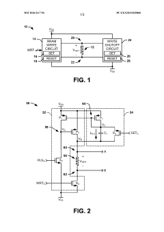
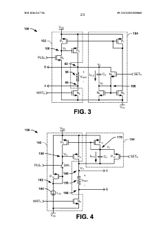
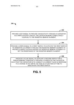
Resistive random access memory (RRAM) system
PatentWO2016167756A1
Innovation
- The RRAM system incorporates a write shutoff circuit that monitors the change in write voltage over time and immediately deactivates the write operation upon detecting a rapid change in resistance, using capacitors and switches to terminate the write stimulus efficiently.
Reliability and Endurance Considerations for Large RRAM Arrays
Reliability and endurance remain critical challenges for the widespread adoption of RRAM technology in large data arrays. Current RRAM devices typically demonstrate endurance levels ranging from 10^5 to 10^9 write cycles, which falls short compared to conventional DRAM (10^15 cycles) and even NAND flash memory (10^4-10^5 cycles for modern 3D NAND). This limitation becomes particularly problematic when quantifying RRAM capacities for big data applications where frequent write operations are expected.
The reliability of RRAM cells in large arrays is affected by several key factors. Variability in switching behavior between cells represents a significant concern, with resistance distributions often showing considerable overlap between ON and OFF states after repeated cycling. This variability increases with array scaling, as smaller device dimensions lead to greater statistical variations in filament formation and rupture processes.
Retention characteristics present another critical consideration for large RRAM arrays. While some RRAM technologies demonstrate excellent data retention exceeding 10 years at 85°C, this performance can degrade significantly after multiple programming cycles. Recent studies have shown that retention failures in large arrays often follow a Weibull distribution, with tail bits exhibiting accelerated degradation that can compromise the integrity of the entire memory block.
Temperature dependency further complicates reliability assessments for RRAM arrays. Operating temperatures can significantly impact both SET and RESET voltages, with higher temperatures generally reducing the energy required for switching but potentially narrowing the operating window. This temperature sensitivity necessitates robust compensation mechanisms when deploying RRAM in varied environmental conditions.
Read disturbance effects represent a subtle but important reliability concern in large arrays. Repeated read operations at voltages below the nominal switching threshold can gradually alter the resistance state of RRAM cells, leading to data corruption over time. This phenomenon becomes more pronounced as array sizes increase, requiring careful consideration of read voltage margins and potential refresh schemes.
Wear-leveling strategies have emerged as essential techniques for extending the effective endurance of large RRAM arrays. Advanced wear-leveling algorithms can distribute write operations more evenly across the array, preventing premature failure of frequently accessed cells. Some recent implementations have demonstrated up to 10x improvement in effective array lifetime through intelligent wear management.
Error correction codes (ECC) specifically optimized for RRAM failure mechanisms have shown promise in enhancing reliability. Multi-bit ECC schemes capable of handling both random and clustered errors can significantly improve the uncorrectable bit error rate (UBER) of large arrays, though at the cost of additional silicon area and power consumption.
Integration Challenges with Conventional Computing Architectures
The integration of RRAM (Resistive Random Access Memory) technology with conventional computing architectures presents significant challenges that must be addressed for successful implementation in large data arrays. Traditional von Neumann architectures, characterized by separate processing and memory units, face fundamental limitations when interfacing with RRAM technology. The memory bottleneck, often referred to as the "von Neumann bottleneck," becomes particularly pronounced when attempting to leverage RRAM's potential for high-density storage in data-intensive applications.
Power management represents another critical integration challenge. While RRAM offers lower power consumption compared to conventional memory technologies, the interface circuitry required for reading and writing operations can introduce significant power overhead. This becomes especially problematic in large data arrays where thousands or millions of RRAM cells must be accessed simultaneously, potentially negating the inherent power advantages of the technology.
Signal integrity issues emerge when integrating RRAM into existing computing frameworks. The variable resistance states that enable RRAM's multi-bit storage capabilities also introduce noise susceptibility and potential signal degradation during read operations. Conventional sensing amplifiers and signal processing circuits must be redesigned to accommodate the unique electrical characteristics of RRAM cells, particularly when scaling to large array sizes.
Addressing schemes present additional complexity. Unlike conventional memory technologies with well-established addressing protocols, RRAM arrays—especially when configured for high-density storage—require specialized addressing mechanisms that can efficiently navigate the three-dimensional structure often employed in advanced RRAM implementations. These addressing schemes must balance access speed with power efficiency while maintaining compatibility with existing system interfaces.
Thermal management considerations cannot be overlooked. RRAM programming operations, particularly those involving filament formation or dissolution, generate localized heating that can affect neighboring cells in densely packed arrays. This thermal crosstalk becomes increasingly problematic as array sizes grow, potentially limiting the practical density achievable in real-world implementations without sophisticated thermal management solutions.
Finally, standardization remains an ongoing challenge. Unlike mature memory technologies with well-established interfaces and protocols, RRAM integration suffers from a lack of industry-wide standards. This fragmentation complicates system design and limits interoperability between different RRAM implementations and conventional computing components, creating barriers to widespread adoption despite the technology's promising capacity characteristics in large data applications.
Unlock deeper insights with Patsnap Eureka Quick Research — get a full tech report to explore trends and direct your research. Try now!
Generate Your Research Report Instantly with AI Agent
Supercharge your innovation with Patsnap Eureka AI Agent Platform!