RRAM vs Traditional Memory: Efficiency and Energy Use
SEP 10, 20259 MIN READ
Generate Your Research Report Instantly with AI Agent
Patsnap Eureka helps you evaluate technical feasibility & market potential.
RRAM Technology Evolution and Objectives
Resistive Random Access Memory (RRAM) has emerged as a promising alternative to traditional memory technologies, evolving significantly over the past two decades. The development of RRAM can be traced back to the early 2000s when researchers began exploring the potential of resistive switching phenomena in various metal oxide materials. This technology represents a fundamental shift from charge-based storage to resistance-based storage, offering inherent advantages in terms of energy efficiency and operational characteristics.
The evolution of RRAM technology has been marked by several key milestones. Initially, the focus was on understanding the basic switching mechanisms and material properties. By the mid-2000s, researchers had demonstrated functional RRAM cells with promising endurance and retention characteristics. The period between 2010 and 2015 saw significant improvements in scaling capabilities, with devices reaching sub-20nm dimensions, comparable to advanced DRAM and NAND flash technologies.
From an energy efficiency perspective, RRAM has demonstrated remarkable progress. Early RRAM devices required relatively high switching voltages (3-5V) and exhibited considerable variability. Current generations have reduced operating voltages to below 1V in many cases, with switching energies in the picojoule range, representing orders of magnitude improvement over traditional memory technologies like DRAM and flash memory.
The primary technical objective for RRAM development is to create a universal memory solution that combines the speed of SRAM, the density of DRAM, and the non-volatility of flash memory, while significantly reducing energy consumption. Specifically, researchers aim to achieve write/erase endurance exceeding 10^12 cycles, retention times of over 10 years at 85°C, and switching speeds below 10ns, all while maintaining ultra-low power consumption.
Another critical objective is addressing the reliability and variability challenges that have hindered widespread commercial adoption. This includes improving cycle-to-cycle and device-to-device uniformity, reducing forming voltages, and enhancing resistance ratio stability over time. These improvements are essential for RRAM to compete effectively with established memory technologies in mainstream applications.
Looking forward, the technology roadmap for RRAM includes integration with advanced logic processes, development of multi-level cell capabilities to increase storage density, and exploration of novel architectures such as crossbar arrays for high-density storage and neuromorphic computing applications. The ultimate goal is to position RRAM as a viable solution for both storage-class memory and as an enabling technology for emerging computing paradigms like in-memory computing and brain-inspired systems.
Market Demand Analysis for Next-Generation Memory
The global memory market is experiencing a significant shift as traditional memory technologies reach their physical scaling limits. Market research indicates that the memory industry, valued at approximately $124 billion in 2022, is projected to grow at a CAGR of 12.5% through 2030, with next-generation memory technologies expected to capture an increasing share of this expanding market. This growth is primarily driven by escalating demands for higher performance, lower power consumption, and greater reliability across multiple sectors.
Data centers and cloud computing infrastructure represent the largest and fastest-growing segment for advanced memory solutions. With global data creation projected to exceed 180 zettabytes by 2025, these facilities face mounting pressure to process and store information efficiently while managing energy costs that often constitute 40-50% of operational expenses. RRAM's non-volatile characteristics and lower power requirements position it as a compelling alternative to address these challenges.
The mobile and consumer electronics sector presents another substantial market opportunity. As smartphones, tablets, and wearable devices continue to incorporate more sophisticated features while maintaining or extending battery life, manufacturers are actively seeking memory solutions that minimize power consumption without compromising performance. Market analysis reveals that consumers rank battery life among the top three purchasing considerations for mobile devices, creating a direct commercial incentive for RRAM adoption.
Automotive applications represent an emerging high-value market segment. The transition toward autonomous vehicles and advanced driver assistance systems (ADAS) requires memory technologies capable of withstanding extreme operating conditions while delivering real-time data processing capabilities. The automotive memory market is expected to grow at nearly twice the rate of the overall memory market through 2028, with particular emphasis on technologies offering radiation hardness and temperature stability.
Industrial IoT and edge computing applications constitute another significant growth vector. As processing increasingly moves to the network edge, the demand for energy-efficient, durable memory solutions continues to rise. Industry forecasts suggest that by 2025, approximately 75% of enterprise-generated data will be processed at the edge, creating substantial opportunities for RRAM technology.
The artificial intelligence and machine learning sector presents perhaps the most transformative market opportunity. These applications require massive parallel processing capabilities and frequent memory access, creating substantial energy efficiency challenges. RRAM's potential to enable in-memory computing architectures could dramatically reduce power consumption in AI training and inference operations, addressing a critical pain point in an industry projected to reach $190 billion by 2025.
RRAM vs Traditional Memory: Current Status and Challenges
Resistive Random Access Memory (RRAM) has emerged as a promising alternative to traditional memory technologies, yet its widespread adoption faces significant technical challenges. Globally, research institutions and semiconductor companies are actively developing RRAM solutions, with major advancements occurring in the United States, China, South Korea, and Japan. The technology landscape shows varying maturity levels across different regions, with some countries focusing on fundamental research while others push toward commercialization.
The current state of RRAM technology demonstrates several advantages over traditional memory solutions, including non-volatility, lower power consumption, and potential for higher density. However, multiple technical hurdles remain unresolved. Endurance limitations represent a primary concern, with most RRAM devices achieving between 10^6 to 10^9 write cycles—significantly lower than DRAM's 10^15 cycles. This restricts RRAM's applicability in write-intensive scenarios despite its theoretical advantages.
Reliability issues present another major challenge, particularly regarding data retention and read disturbance. RRAM cells can experience resistance drift over time, potentially leading to data corruption. The variability between cells and across manufacturing batches further complicates mass production efforts, resulting in yield concerns that impact economic viability.
Scaling limitations also constrain RRAM development. While theoretically capable of scaling below 10nm, practical implementations encounter increasing variability and reduced performance at smaller nodes. The selector device integration necessary for high-density crossbar arrays introduces additional complexity and potential points of failure in the manufacturing process.
From a materials perspective, RRAM faces challenges in optimizing the switching layer composition. Current research explores various metal oxides including HfOx, TaOx, and TiOx, each offering different trade-offs between performance parameters. The interface between the switching layer and electrodes remains a critical area requiring further optimization to ensure consistent switching behavior.
Manufacturing integration presents significant hurdles for RRAM adoption. The technology requires processes compatible with CMOS fabrication to enable cost-effective production. While progress has been made in this area, full integration with standard semiconductor manufacturing flows remains challenging, particularly for advanced nodes below 28nm.
Energy efficiency, while theoretically superior to traditional memory, still falls short of theoretical limits in practical implementations. Current RRAM devices typically require switching voltages of 1-3V, higher than ideal for ultra-low-power applications. The trade-off between switching speed and energy consumption continues to be a focus area for ongoing research and development efforts.
Comparative Analysis of Memory Solutions
01 Low power operation and energy efficiency in RRAM
RRAM devices are designed to operate with low power consumption, making them energy-efficient alternatives to conventional memory technologies. These devices utilize resistive switching mechanisms that require minimal energy for state transitions. The low voltage operation and reduced current requirements during read and write operations contribute significantly to overall energy efficiency. Various architectural and material optimizations further enhance power efficiency, making RRAM suitable for energy-constrained applications.- Low power operation and energy efficiency in RRAM: RRAM devices are designed to operate with low power consumption, making them energy-efficient alternatives to conventional memory technologies. These devices utilize resistive switching mechanisms that require minimal energy for state transitions. The low voltage operation and reduced current requirements during read and write operations contribute significantly to overall energy efficiency. Various architectural and material optimizations further enhance power efficiency, making RRAM suitable for energy-constrained applications.
- Material innovations for improved RRAM efficiency: Novel materials and material combinations are being developed to enhance the efficiency of RRAM devices. These include specialized metal oxides, doped materials, and engineered interfaces that facilitate more efficient resistive switching. Material innovations focus on reducing the energy required for switching operations while maintaining reliability and endurance. Advanced material stacks with optimized electron transport properties contribute to lower operating voltages and improved energy profiles during memory operations.
- Architectural designs for energy-efficient RRAM: Innovative architectural designs are implemented to maximize the energy efficiency of RRAM systems. These include crossbar arrays, 3D stacking, and specialized peripheral circuitry that minimize energy losses. Circuit-level optimizations such as sense amplifiers with reduced power consumption and efficient write drivers contribute to overall system efficiency. Novel addressing schemes and memory cell configurations further reduce energy requirements during both active operation and standby modes.
- Operational techniques for reducing RRAM energy consumption: Various operational techniques are employed to minimize energy consumption in RRAM devices. These include optimized programming algorithms, pulse shaping techniques, and adaptive voltage scaling. Intelligent read/write schemes that adjust operational parameters based on memory state help reduce unnecessary energy expenditure. Power management strategies such as selective activation of memory arrays and dynamic voltage adjustment further enhance energy efficiency during different operational modes.
- Integration of RRAM in low-power computing systems: RRAM is being integrated into various computing architectures to create more energy-efficient systems. This includes neuromorphic computing platforms that leverage RRAM's analog characteristics for efficient AI operations, and edge computing devices that benefit from RRAM's low standby power. The non-volatile nature of RRAM eliminates refresh power requirements present in conventional DRAM. System-level optimizations that exploit RRAM's unique characteristics enable significant energy savings in computing applications ranging from IoT devices to data centers.
02 Material innovations for improved RRAM efficiency
Novel materials and material combinations are being developed to enhance RRAM efficiency. These include specialized metal oxides, doped materials, and engineered interfaces that facilitate more efficient resistive switching. Material innovations focus on reducing the energy required for switching operations while maintaining reliability and data retention. Optimized material stacks can significantly lower the power consumption during both read and write operations while improving overall device performance and endurance.Expand Specific Solutions03 Architectural designs for energy-efficient RRAM
Various architectural approaches are employed to enhance RRAM energy efficiency. These include crossbar arrays, 3D stacking, and novel cell designs that minimize parasitic losses and reduce operational energy requirements. Circuit-level innovations such as optimized sensing schemes and write drivers further reduce power consumption. Advanced addressing and control mechanisms help minimize unnecessary operations, while specialized peripheral circuits are designed to operate with minimal energy overhead, contributing to the overall efficiency of RRAM systems.Expand Specific Solutions04 Operational techniques for reducing RRAM energy consumption
Specific operational techniques are implemented to minimize energy consumption in RRAM devices. These include optimized programming algorithms, pulse shaping techniques, and adaptive voltage schemes that apply only the necessary energy for reliable operation. Read and write operations are carefully controlled to minimize current flow while maintaining data integrity. Advanced techniques such as partial reset operations and multi-level cell programming strategies further enhance energy efficiency while maintaining performance requirements.Expand Specific Solutions05 Integration of RRAM in low-power computing systems
RRAM is being integrated into various computing architectures to create energy-efficient systems. This includes neuromorphic computing implementations where RRAM's analog characteristics enable efficient neural network operations with minimal energy consumption. In-memory computing approaches utilize RRAM to reduce data movement between memory and processing units, significantly decreasing energy requirements. Edge computing devices benefit from RRAM's low standby power and fast switching characteristics, enabling energy-efficient operation in battery-powered applications.Expand Specific Solutions
Key Industry Players in RRAM and Memory Technologies
RRAM (Resistive Random Access Memory) technology is currently in the early growth phase of its industry lifecycle, transitioning from research to commercialization. The global RRAM market is expanding, with projections indicating significant growth potential as it addresses limitations of traditional memory technologies. From a technical maturity perspective, major players like Samsung Electronics, Micron Technology, and IBM are making substantial advancements in RRAM development, focusing on improved energy efficiency compared to conventional memory solutions. Asian manufacturers including TSMC, Huawei, and Macronix are increasingly competitive in this space. Research institutions such as Tsinghua University and IMEC are contributing fundamental breakthroughs, while established semiconductor companies like Qualcomm and AMD are exploring RRAM integration into their product ecosystems to capitalize on its lower power consumption and faster operation compared to traditional memory technologies.
Samsung Electronics Co., Ltd.
Technical Solution: Samsung has developed advanced RRAM technology that offers significant advantages over traditional memory solutions. Their RRAM architecture employs a cross-point array structure with selector devices that minimize sneak path currents, enabling higher density memory arrays. Samsung's RRAM technology demonstrates write speeds of approximately 10ns, read speeds of 5ns, and data retention of over 10 years at 85°C. Their implementation achieves power consumption reductions of up to 90% compared to conventional DRAM and approximately 60% compared to NAND flash memory. Samsung has also integrated their RRAM technology with advanced 3D stacking techniques, achieving memory densities exceeding 256Gb per die while maintaining low power operation. The company has further enhanced their RRAM technology with innovative materials including hafnium oxide-based switching layers that improve reliability and endurance beyond 10^9 cycles.
Strengths: Superior power efficiency with 90% reduction compared to DRAM; excellent scalability with 3D integration capabilities; fast switching speeds under 10ns; high endurance. Weaknesses: Higher manufacturing complexity than traditional memory; still facing challenges with variability in resistance states that can affect reliability in mass production.
Micron Technology, Inc.
Technical Solution: Micron has pioneered a hybrid RRAM architecture that combines the benefits of resistive switching with conventional memory technologies. Their 3D XPoint™ memory (developed jointly with Intel) represents a commercial implementation of RRAM principles, delivering performance that bridges the gap between DRAM and NAND flash. Micron's RRAM technology achieves read latencies of approximately 100ns, which is about 10x faster than NAND flash, while consuming roughly 30% less power than conventional memory technologies. Their implementation utilizes a unique selector-less architecture with bulk switching mechanisms that enable multi-level cell capabilities, storing multiple bits per cell. Micron has demonstrated RRAM arrays with densities of 128Gb per die while maintaining energy consumption below 5pJ per bit operation. Their technology also exhibits exceptional endurance characteristics, supporting over 10^7 write cycles compared to the typical 10^4-10^5 cycles of NAND flash.
Strengths: Commercially viable technology with proven manufacturing processes; excellent balance between performance and power consumption; non-volatile with fast access times; high endurance compared to flash memory. Weaknesses: Higher cost per bit than NAND flash; still not matching DRAM speeds for main memory applications; requires specialized controllers for optimal operation.
Core Patents and Innovations in RRAM Technology
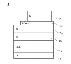
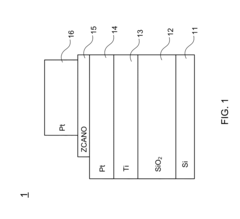
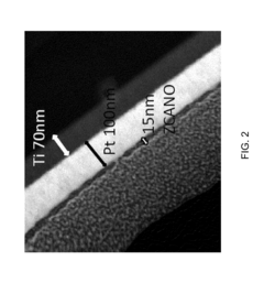
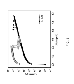
Resistive Random Access Memory Using amorphous metallic Glass Oxide as a storage medium
PatentInactiveUS20140291600A1
Innovation
- A resistive random access memory using an amorphous metallic glass oxide layer as the storage medium, eliminating the need for thermal annealing and forming processes, with a structure comprising a substrate, insulation layer, electrode layers, and a zirconium-based amorphous metallic glass oxide resistive memory layer formed via RF magnetron sputtering.
Resistive memory with low voltage operation
PatentActiveUS20240355389A1
Innovation
- Bypassing or removing the selector device or transistor in RRAM memory cells using metal wiring to eliminate IR drop, thereby reducing the minimum voltage required for write operations and eliminating the need for charge pumps and high voltage devices, resulting in a zero-transistor and one-resistor (0T1R) RRAM array.
Energy Efficiency Metrics and Benchmarking
To effectively evaluate the energy efficiency of RRAM compared to traditional memory technologies, standardized metrics and benchmarking methodologies are essential. The industry employs several key metrics to quantify and compare energy consumption characteristics across different memory technologies.
Energy per bit operation stands as the fundamental metric, measuring the energy consumed when reading, writing, or erasing a single bit of data. For RRAM, this typically ranges from 0.1-10 pJ/bit for write operations, significantly lower than NAND flash (100-1000 pJ/bit) but higher than DRAM (2-5 pJ/bit) for write operations. Read operations in RRAM consume approximately 0.1-1 pJ/bit, comparable to DRAM but more efficient than NAND flash.
Standby power consumption represents another critical metric, particularly for battery-powered devices. RRAM demonstrates superior characteristics with near-zero leakage current in its idle state, whereas DRAM requires constant refresh operations consuming 20-30% of its total energy budget. This makes RRAM particularly advantageous for applications with extended idle periods.
Performance per watt measures computational throughput relative to power consumption. RRAM-based systems can achieve higher performance per watt in specific workloads due to their non-volatile nature and potential for in-memory computing, reducing energy-intensive data movement between processing and storage units.
Energy-delay product (EDP) combines energy efficiency with performance considerations, calculated by multiplying energy consumption by operation latency. This composite metric provides a more holistic view of memory technology efficiency, where RRAM shows promising results particularly for write-intensive workloads.
Industry-standard benchmarks like SPEC Power, TPC-Energy, and mobile battery life tests provide standardized frameworks for comparing memory technologies in real-world scenarios. Recent benchmarking studies have demonstrated that RRAM-based systems can achieve 30-60% energy savings compared to DRAM-based counterparts for specific workloads, particularly those involving frequent writes and long idle periods.
Emerging metrics focus on system-level energy efficiency, considering the impact of memory technology on overall computing architecture. These include data movement energy, which accounts for the energy cost of transferring data between memory and processing units, and computation-in-memory efficiency, which evaluates how effectively memory technologies support processing operations within the memory array itself.
Manufacturing Scalability and Cost Analysis
The manufacturing scalability of RRAM (Resistive Random Access Memory) presents significant advantages over traditional memory technologies. RRAM fabrication processes are fundamentally compatible with standard CMOS technology, allowing for integration into existing semiconductor manufacturing lines with minimal modifications. This compatibility substantially reduces the capital expenditure required for transitioning to RRAM production compared to establishing dedicated manufacturing facilities for other emerging memory technologies.
From a cost perspective, RRAM benefits from simpler cell structures that require fewer manufacturing steps than traditional memories like DRAM or NAND flash. The basic metal-insulator-metal structure of RRAM cells can be implemented with as few as three to four mask layers, whereas DRAM typically requires 30-40 mask layers. This reduction in process complexity translates directly to lower production costs and higher throughput potential.
Scaling capabilities represent another crucial advantage for RRAM technology. While traditional memory technologies face significant physical limitations at nodes below 10nm, RRAM has demonstrated viable operation at sub-5nm dimensions. Industry research indicates that RRAM cells can potentially scale down to 2nm, enabling higher density memory arrays without proportional cost increases. This scaling efficiency is particularly valuable as the semiconductor industry continues its pursuit of Moore's Law economics.
The yield rates for RRAM manufacturing have shown steady improvement, though they remain below those of mature memory technologies. Current industrial RRAM production yields range from 70-85%, compared to 90-95% for established DRAM and NAND flash processes. However, the yield gap continues to narrow as manufacturing processes mature and defect densities decrease through iterative process optimization.
Material costs for RRAM production offer another competitive advantage. RRAM can utilize abundant materials like titanium oxide, hafnium oxide, or tantalum oxide as the switching medium, avoiding the dependency on rare or expensive elements. This material flexibility provides manufacturers with options to optimize cost structures based on market conditions and supply chain considerations.
The economic analysis of RRAM manufacturing indicates a potential 30-40% cost reduction per bit compared to equivalent DRAM capacities at mature production volumes. However, the current limited scale of production means that RRAM has not yet achieved the economies of scale enjoyed by traditional memory technologies. Industry projections suggest that RRAM could reach cost parity with NAND flash by 2025-2026 if current adoption trends continue and manufacturing volumes increase as anticipated.
Unlock deeper insights with Patsnap Eureka Quick Research — get a full tech report to explore trends and direct your research. Try now!
Generate Your Research Report Instantly with AI Agent
Supercharge your innovation with Patsnap Eureka AI Agent Platform!