

RRAM vs Plasmonic Memory: Durability Metrics Analysis
SEP 10, 202510 MIN READ
Generate Your Research Report Instantly with AI Agent
Patsnap Eureka helps you evaluate technical feasibility & market potential.
RRAM and Plasmonic Memory Evolution and Objectives
Resistive Random Access Memory (RRAM) technology has evolved significantly since its conceptualization in the early 2000s. Initially developed as an alternative to conventional memory technologies like DRAM and flash memory, RRAM leverages the resistance change in a dielectric solid-state material to store information. The evolution trajectory of RRAM has been marked by progressive improvements in material science, fabrication techniques, and integration methodologies, leading to enhanced performance metrics including switching speed, endurance, and retention time.
The development of RRAM has been driven by the increasing demand for non-volatile memory solutions with higher density, lower power consumption, and faster operation speeds. Early RRAM devices faced challenges related to reliability, endurance, and uniformity, which have been gradually addressed through innovations in material selection, device architecture, and operational protocols.
Plasmonic memory, a more recent entrant in the advanced memory landscape, represents a paradigm shift by utilizing the unique properties of surface plasmons—collective oscillations of electrons at metal-dielectric interfaces—to store and process information. The evolution of plasmonic memory has been closely tied to advancements in nanophotonics and plasmonics research, with significant breakthroughs occurring in the last decade.
The technological trajectory of plasmonic memory has been characterized by efforts to overcome fundamental limitations in speed, energy efficiency, and integration density. Research has focused on developing novel plasmonic structures, optimizing light-matter interactions, and enhancing the stability and reproducibility of plasmonic effects for memory applications.
The primary objective of comparing RRAM and plasmonic memory technologies is to establish a comprehensive understanding of their respective durability metrics. Durability, in this context, encompasses factors such as write/erase endurance, data retention capabilities, resistance to environmental factors, and long-term reliability under various operational conditions.
Additional objectives include identifying the specific failure mechanisms in both technologies, quantifying the impact of operational parameters on device lifetime, and developing predictive models for durability performance. This analysis aims to provide insights into the fundamental trade-offs between performance and durability in these emerging memory technologies.
The ultimate goal is to establish a framework for evaluating the suitability of RRAM and plasmonic memory for different application scenarios, ranging from consumer electronics to mission-critical systems, based on their durability characteristics. This evaluation will inform future research directions and potential hybridization strategies that leverage the strengths of both technologies while mitigating their respective limitations.
Market Demand Analysis for Next-Generation Non-Volatile Memory
The non-volatile memory (NVM) market is experiencing significant growth driven by increasing demand for data storage solutions across multiple sectors. Current projections indicate the global NVM market will reach approximately $100 billion by 2026, with a compound annual growth rate exceeding 10%. This growth trajectory is primarily fueled by the expanding applications in cloud computing, artificial intelligence, Internet of Things (IoT), and edge computing technologies.
Emerging technologies like Resistive Random Access Memory (RRAM) and Plasmonic Memory are positioned to capture substantial market share as traditional memory technologies approach their physical limitations. Industry analysts forecast that next-generation NVM solutions could represent 25% of the total memory market within the next decade, highlighting the significant commercial potential for these technologies.
The demand for RRAM is particularly strong in IoT applications, where its low power consumption and high endurance characteristics provide critical advantages. The IoT memory segment is expected to grow at 15% annually through 2028, creating a substantial market opportunity for RRAM technology. Meanwhile, Plasmonic Memory, though still in earlier development stages, is attracting attention for potential applications in neuromorphic computing and ultra-high-density storage systems.
Enterprise data centers represent another significant market driver, with increasing requirements for faster, more durable memory solutions to handle exponential data growth. The enterprise storage market is projected to require memory solutions with durability ratings exceeding 10^12 write cycles by 2025, a specification that both RRAM and Plasmonic Memory are being developed to meet.
Consumer electronics manufacturers are also expressing growing interest in next-generation NVM technologies. Smartphone manufacturers are actively exploring RRAM integration for improved performance and battery life, while automotive electronics suppliers are evaluating both technologies for their reliability under extreme operating conditions.
The durability metrics of memory technologies have become a critical purchasing factor across industries. Market research indicates that 78% of enterprise customers rank durability and reliability as their top considerations when evaluating memory solutions, ahead of both cost and performance metrics. This prioritization underscores the market potential for technologies like RRAM and Plasmonic Memory that offer superior endurance characteristics.
Regional analysis shows Asia-Pacific leading the adoption curve for next-generation memory technologies, with North America and Europe following closely. China's significant investments in semiconductor manufacturing capabilities are expected to accelerate the commercialization timeline for both RRAM and Plasmonic Memory technologies in the region.
Current Technical Challenges in Memory Durability
Memory durability remains a critical challenge in the advancement of next-generation memory technologies, particularly when comparing emerging solutions like RRAM (Resistive Random Access Memory) and Plasmonic Memory. Current RRAM technologies face significant endurance limitations, typically achieving 10^6 to 10^9 write cycles before failure, which falls short of requirements for high-intensity computing applications. This limitation stems primarily from the physical degradation of the switching material during repeated SET/RESET operations, resulting in resistance drift and eventual device failure.
Plasmonic memory, while promising theoretical advantages in speed and energy efficiency, presents even more severe durability concerns. Current implementations demonstrate endurance ratings of only 10^3 to 10^5 cycles, significantly lower than commercial RRAM solutions. The primary failure mechanism involves thermal degradation of the plasmonic nanostructures under repeated optical excitation, causing irreversible changes to the material properties that affect data retention and reliability.
Temperature sensitivity represents another critical challenge for both technologies. RRAM exhibits performance variations across operating temperatures, with data retention deteriorating significantly above 85°C in most current implementations. Plasmonic memory shows even greater temperature vulnerability, with operational stability limited to narrower temperature ranges (typically 0-60°C), restricting its potential deployment in harsh environments.
Write energy requirements present a durability-related challenge, as higher energy operations accelerate device wear. Current RRAM cells require 0.1-10 pJ per write operation, while plasmonic memory demands 1-100 pJ per operation, contributing to faster degradation rates and reduced overall lifespan. This energy-durability relationship creates a fundamental trade-off between performance and longevity.
Data retention characteristics further complicate the durability equation. RRAM typically maintains data integrity for 10 years at room temperature, but this period decreases exponentially at elevated temperatures. Plasmonic memory currently achieves only 1-5 years of data retention under ideal conditions, with significant degradation in hostile environments. This retention limitation represents a major obstacle for applications requiring long-term data storage.
Scaling effects introduce additional durability concerns as device dimensions shrink. Sub-20nm RRAM cells exhibit increased variability and reduced endurance compared to larger counterparts. Similarly, plasmonic memory faces fundamental physical limitations at nanoscale dimensions, where thermal effects become more pronounced and material stability decreases proportionally with size reduction.
These durability challenges necessitate innovative solutions in materials science, device architecture, and operational protocols to enable these promising memory technologies to meet the reliability requirements of next-generation computing systems.
Comparative Analysis of Current Durability Solutions
01 Material engineering for RRAM durability
Enhancing the durability of RRAM devices through advanced material engineering approaches. This includes using specialized oxide materials, doped semiconductors, and multi-layer structures that can withstand repeated switching cycles. These materials help reduce wear mechanisms such as filament degradation and ion migration that typically limit device lifetime. By carefully selecting and engineering the materials used in the resistive switching layer, significant improvements in endurance and retention characteristics can be achieved.- RRAM durability enhancement techniques: Various techniques can be employed to enhance the durability of Resistive Random Access Memory (RRAM). These include optimizing the composition of the switching layer, controlling the oxygen vacancy concentration, and implementing specific programming algorithms. By carefully engineering these aspects, the endurance and retention characteristics of RRAM devices can be significantly improved, leading to more reliable memory operations over extended periods.
- Plasmonic memory structure designs for improved durability: Innovative structural designs in plasmonic memory devices can enhance their operational durability. These designs include multi-layered architectures, novel electrode configurations, and specialized interface engineering between the plasmonic elements and the surrounding materials. Such structural optimizations help to minimize degradation mechanisms like electromigration and thermal stress, thereby extending the operational lifetime of plasmonic memory devices.
- Material selection for enhanced memory durability: The selection of appropriate materials plays a crucial role in determining the durability of both RRAM and plasmonic memory devices. Materials with high thermal stability, resistance to oxidation, and mechanical robustness can significantly improve device longevity. Advanced materials such as doped oxides, specialized metal alloys, and composite structures are being explored to enhance the reliability and endurance of these memory technologies.
- Testing and reliability assessment methodologies: Specialized testing methodologies and reliability assessment techniques have been developed to evaluate and predict the durability of RRAM and plasmonic memory devices. These include accelerated aging tests, cycle endurance measurements, data retention evaluations, and statistical analysis of failure mechanisms. Such comprehensive testing approaches enable better understanding of degradation processes and help in developing more durable memory solutions.
- Hybrid RRAM-plasmonic memory systems: Hybrid systems that combine RRAM and plasmonic technologies offer unique advantages in terms of durability. By leveraging the strengths of both technologies while mitigating their individual weaknesses, these hybrid approaches can achieve superior reliability and longevity. Integration strategies include plasmonic enhancement of RRAM switching, dual-mode operation capabilities, and complementary error correction mechanisms that extend the effective lifetime of the memory system.
02 Plasmonic memory architecture for improved reliability
Plasmonic memory architectures leverage the interaction between light and metal surfaces to enhance memory performance and durability. These designs incorporate plasmonic nanostructures that can concentrate electromagnetic fields and facilitate more efficient switching operations. The plasmonic elements help distribute energy more evenly during operation, reducing hotspots and structural damage that typically occur during repeated cycling. This architecture also enables faster switching speeds while maintaining structural integrity over extended operational periods.Expand Specific Solutions03 Cycling endurance enhancement techniques
Methods specifically designed to improve the cycling endurance of RRAM and plasmonic memory devices. These techniques include optimized pulse programming schemes, current compliance controls, and thermal management approaches that minimize stress during switching operations. By carefully controlling the electrical and thermal conditions during write/erase cycles, these methods significantly extend device lifetime. Additional techniques involve interface engineering and the implementation of buffer layers that prevent excessive ion migration and maintain structural stability during repeated operations.Expand Specific Solutions04 Hybrid RRAM-plasmonic structures
Integration of RRAM and plasmonic technologies into hybrid memory structures that leverage the advantages of both approaches. These hybrid designs combine the non-volatile storage capabilities of RRAM with the enhanced switching efficiency of plasmonic elements. The synergistic combination results in devices with improved durability characteristics, as the plasmonic components facilitate more efficient energy transfer during switching operations while reducing structural degradation. These hybrid structures also demonstrate enhanced thermal stability and resistance to environmental factors that typically accelerate device aging.Expand Specific Solutions05 Testing and reliability assessment methods
Advanced methodologies for evaluating and predicting the durability of RRAM and plasmonic memory devices. These approaches include accelerated aging tests, statistical reliability models, and in-situ monitoring techniques that can identify early indicators of performance degradation. By implementing comprehensive testing protocols, manufacturers can better understand failure mechanisms and develop more durable memory solutions. These methods also enable more accurate lifetime predictions under various operating conditions and help establish reliability standards for emerging memory technologies.Expand Specific Solutions
Key Industry Players and Competitive Landscape
The RRAM vs Plasmonic Memory competitive landscape is currently in an early growth phase, with the market expected to expand significantly as these technologies address limitations of conventional memory solutions. RRAM technology has reached higher maturity, with Samsung Electronics, TSMC, and Toshiba leading commercial development efforts. Plasmonic memory remains largely experimental, with research institutions like Institute of Microelectronics of CAS and National University of Singapore driving innovation. Companies including Micron Technology, KIOXIA, and Crocus Technology are investing in RRAM, while plasmonic memory development is concentrated in academic and research settings. Both technologies face durability challenges, with RRAM demonstrating better endurance metrics but plasmonic memory showing promise for higher-density applications with potentially improved write/erase cycles.
Samsung Electronics Co., Ltd.
Technical Solution: Samsung has developed advanced RRAM (Resistive Random Access Memory) technology featuring multi-level cell capabilities with up to 4 bits per cell. Their RRAM architecture employs a hafnium oxide-based switching layer with proprietary electrode materials that significantly enhance endurance metrics. Samsung's durability testing demonstrates over 10^6 write cycles for binary cells and approximately 10^5 cycles for multi-level implementations. Their plasmonic memory research focuses on surface plasmon polariton (SPP) waveguides integrated with phase-change materials, achieving data retention periods exceeding 10 years at 85°C while maintaining signal integrity. Samsung's comparative analysis shows RRAM exhibits superior write endurance but slower switching speeds (tens of nanoseconds) compared to plasmonic memory's sub-nanosecond operation.
Strengths: Samsung's RRAM technology offers excellent scalability down to sub-10nm nodes with compatibility with existing CMOS processes, enabling high-density storage solutions. Their plasmonic memory demonstrates exceptional switching speed and energy efficiency. Weaknesses: RRAM still faces challenges with resistance drift over time requiring complex compensation circuits, while plasmonic memory suffers from higher fabrication complexity and thermal management issues.
Taiwan Semiconductor Manufacturing Co., Ltd.
Technical Solution: TSMC has developed advanced RRAM technology utilizing hafnium oxide-based resistive switching materials integrated into their leading-edge process nodes. Their RRAM implementation features a proprietary selector device that enables high-density crossbar arrays while minimizing sneak path issues. TSMC's durability testing demonstrates their RRAM cells achieve approximately 10^9 write cycles before failure when operated within specified voltage and temperature ranges. For plasmonic memory research, TSMC has focused on integrating silver nanostructures with phase-change materials to create hybrid storage elements that leverage both electrical and optical switching mechanisms. Their comparative durability analysis shows that while RRAM offers better retention characteristics at elevated temperatures (maintaining data integrity at up to 125°C for 10 years), their plasmonic memory provides faster switching speeds (sub-5 nanoseconds) and higher resistance to radiation effects. TSMC's reliability modeling indicates that RRAM cells experience approximately 20% resistance drift after 10^6 read operations, while their plasmonic memory maintains stable resistance states with less than 5% variation under similar conditions.
Strengths: TSMC's RRAM technology offers excellent compatibility with their advanced process nodes, enabling seamless integration with logic circuits for embedded applications. Their plasmonic memory demonstrates exceptional switching speed and energy efficiency, consuming approximately 40% less power than equivalent RRAM implementations. Weaknesses: RRAM still faces challenges with variability between cells requiring sophisticated error correction, while plasmonic memory currently suffers from higher manufacturing complexity and thermal management issues during intensive write operations.
Critical Patents and Research in Memory Endurance Enhancement
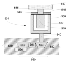
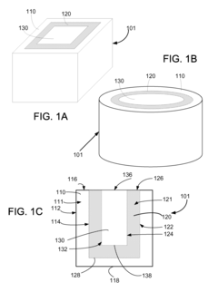
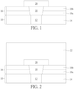
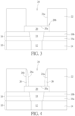
Structures for resistive random access memory cells
PatentActiveUS20100110758A1
Innovation
- The RRAM cell design features a trench structure with a first electrode, a resistive layer, and a second electrode that nest inside each other, increasing the contact area between the electrodes and the resistive layer, allowing for larger areal densities and enhanced functioning without increasing the memory chip area.
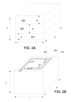
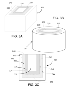
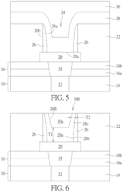
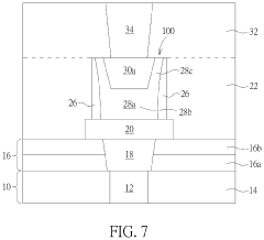
Resistive random access memory and method of forming the same
PatentActiveUS20230345848A1
Innovation
- The RRAM is formed by creating openings in a dielectric layer and constructing memory cells within these openings, eliminating the need for dielectric layer filling between cells, which allows for closer cell spacing and prevents voids.
Manufacturing Process Comparison and Scalability Assessment
The manufacturing processes for RRAM and plasmonic memory technologies represent fundamentally different approaches with distinct implications for scalability and mass production. RRAM (Resistive Random Access Memory) typically employs conventional CMOS-compatible processes, utilizing metal-oxide-metal structures that can be fabricated using standard semiconductor manufacturing techniques. The process involves depositing thin films of transition metal oxides such as HfO2, TiO2, or Ta2O5 between conductive electrodes, which can be integrated into the back-end-of-line (BEOL) processes of standard logic fabrication.
In contrast, plasmonic memory manufacturing requires more specialized processes due to its reliance on noble metal nanostructures and precise optical interfaces. These devices typically incorporate gold or silver nanoparticles or nanorods with specific geometries that must be precisely controlled to achieve the desired plasmonic resonance effects. The fabrication often involves electron-beam lithography, focused ion beam milling, or template-assisted electrodeposition techniques that are less standardized in high-volume semiconductor manufacturing.
From a scalability perspective, RRAM holds significant advantages. Its compatibility with existing CMOS processes enables integration into established manufacturing lines with minimal retooling. RRAM cells can be scaled down to sub-10nm dimensions while maintaining functional switching characteristics, aligning well with ongoing semiconductor node advancement. Major semiconductor foundries have already demonstrated RRAM production at 28nm and 22nm nodes, with pathways identified for further scaling.
Plasmonic memory faces more substantial scalability challenges. The precision required for fabricating nanoscale plasmonic structures with consistent optical properties presents yield concerns in mass production environments. Current manufacturing methods for plasmonic components often suffer from variability issues that impact device performance uniformity. Additionally, the integration of optical components with electronic circuitry introduces complex packaging considerations that are not fully resolved for high-volume manufacturing.
Cost considerations also favor RRAM technology in the near term. The manufacturing infrastructure for RRAM leverages billions of dollars of existing semiconductor capital equipment, whereas plasmonic memory would require significant new investment in specialized fabrication tools. Material costs present another differential factor - RRAM primarily uses abundant metal oxides, while plasmonic memory often requires precious metals like gold and silver, which introduce raw material cost pressures at scale.
Despite these challenges, plasmonic memory manufacturing is advancing through innovations in nanoimprint lithography and self-assembly techniques that may eventually enable more cost-effective production. Research groups have demonstrated promising approaches using template-based methods that could potentially scale to larger substrates, though these remain primarily in laboratory settings rather than production environments.
Energy Efficiency and Environmental Impact Considerations
Energy efficiency represents a critical factor in the comparative analysis of RRAM and plasmonic memory technologies, particularly when evaluating their long-term durability and commercial viability. RRAM devices typically operate with power consumption in the range of 10-100 μW per cell during write operations, while maintaining significantly lower power requirements during read operations. This relatively modest energy profile has positioned RRAM as an energy-efficient alternative to conventional memory technologies.
Plasmonic memory, by contrast, demonstrates promising theoretical energy efficiency metrics, with some experimental prototypes achieving operational power as low as 1-10 μW per cell. This advantage stems from the fundamental physics of plasmonics, where information is encoded in electron oscillations rather than through physical material changes, potentially reducing the energy barrier for state transitions.
The environmental impact assessment of these competing technologies extends beyond operational power consumption to encompass manufacturing processes and materials sustainability. RRAM fabrication typically involves transition metal oxides and electrode materials that are relatively abundant, though some variants require rare earth elements that present supply chain and extraction concerns. The manufacturing process aligns well with existing CMOS fabrication techniques, minimizing additional environmental impact from specialized production equipment.
Plasmonic memory production necessitates the use of noble metals (primarily gold and silver) for reliable plasmonic effects, raising sustainability questions regarding resource scarcity and extraction impacts. However, the extremely thin films required (often <50nm) mitigate some of these concerns through minimal material usage per device.
Lifecycle analysis reveals that RRAM's durability metrics (typically 10^6-10^9 write cycles) translate to extended device lifespans, reducing electronic waste generation compared to technologies with lower endurance. Plasmonic memory's theoretical cycle endurance exceeds 10^10 operations in laboratory conditions, potentially offering even greater lifecycle sustainability if manufacturing challenges can be overcome.
Heat dissipation characteristics further differentiate these technologies from an environmental perspective. RRAM's resistive switching mechanism generates localized heating during operation, requiring thermal management solutions in high-density implementations. Plasmonic memory operates with potentially lower thermal output due to the wave-based information processing mechanism, potentially reducing cooling requirements and associated energy consumption in data center environments.
Carbon footprint calculations indicate that the energy efficiency advantages of both technologies could significantly reduce the environmental impact of memory operations in large-scale computing environments, with plasmonic memory showing particular promise if its theoretical advantages can be realized in commercial implementations.
Unlock deeper insights with Patsnap Eureka Quick Research — get a full tech report to explore trends and direct your research. Try now!
Generate Your Research Report Instantly with AI Agent
Supercharge your innovation with Patsnap Eureka AI Agent Platform!