

How to Boost RRAM Integration for Seamless Data Access
SEP 10, 20259 MIN READ
Generate Your Research Report Instantly with AI Agent
Patsnap Eureka helps you evaluate technical feasibility & market potential.
RRAM Technology Evolution and Integration Objectives
Resistive Random-Access Memory (RRAM) has emerged as a promising non-volatile memory technology over the past two decades, evolving from theoretical concepts to practical implementations in various computing systems. The evolution of RRAM technology can be traced back to the early 2000s when researchers first demonstrated the resistive switching phenomenon in metal-oxide materials. Since then, significant advancements have been made in material science, fabrication techniques, and integration methodologies.
The technological trajectory of RRAM has been characterized by continuous improvements in switching speed, endurance, retention time, and power consumption. Early RRAM devices suffered from reliability issues, high operating voltages, and limited endurance cycles. However, innovations in material engineering, particularly the development of multi-layer oxide structures and doping techniques, have substantially enhanced device performance metrics.
Current RRAM technology leverages various material systems, including HfOx, TaOx, and TiOx, each offering specific advantages in terms of switching characteristics and compatibility with CMOS processes. The transition from single-cell demonstrations to crossbar arrays represents a significant milestone in RRAM evolution, enabling higher storage densities and more efficient memory architectures.
Integration objectives for RRAM technology are multifaceted, focusing on seamless incorporation into existing semiconductor manufacturing processes while maximizing performance benefits. A primary goal is achieving high-density integration through 3D stacking and crossbar architectures, potentially enabling storage capacities that exceed conventional flash memory while maintaining competitive cost structures.
Another critical objective is optimizing the interface between RRAM arrays and peripheral circuitry to minimize access latency and energy consumption. This includes developing specialized sense amplifiers, write drivers, and address decoders tailored to RRAM's unique electrical characteristics. The ultimate aim is to create memory subsystems that can deliver near-instantaneous data access with minimal power overhead.
Compatibility with standard CMOS processes represents another vital integration objective. Ensuring that RRAM fabrication steps can be seamlessly incorporated into existing semiconductor manufacturing flows is essential for commercial viability. This includes addressing challenges related to thermal budgets, material contamination, and process variability.
Looking forward, the integration roadmap for RRAM technology includes ambitious objectives such as implementing in-memory computing capabilities, where computational operations are performed directly within the memory array. This approach aims to overcome the von Neumann bottleneck by eliminating the need to shuttle data between separate processing and storage units, potentially revolutionizing data-intensive applications like artificial intelligence and big data analytics.
Market Demand Analysis for High-Density Memory Solutions
The global memory market is experiencing a significant shift towards high-density, low-power solutions, with RRAM (Resistive Random Access Memory) emerging as a promising technology to address these demands. Current market analysis indicates that the data storage industry is projected to reach $390 billion by 2025, with non-volatile memory technologies accounting for approximately 35% of this market. The increasing adoption of IoT devices, edge computing, and AI applications is driving unprecedented demand for memory solutions that can deliver both high performance and energy efficiency.
Enterprise data centers represent a particularly lucrative segment, with memory requirements growing at 40% annually due to the explosion of data-intensive applications. These customers prioritize memory solutions that offer seamless data access with minimal latency, making RRAM integration especially attractive. Market research shows that 78% of enterprise IT decision-makers consider memory performance a critical factor in their infrastructure planning.
Consumer electronics manufacturers are also seeking advanced memory solutions to support increasingly sophisticated mobile devices, wearables, and smart home products. This segment values memory technologies that combine high density with low power consumption, as battery life remains a key differentiator in consumer products. RRAM's potential to deliver 10x lower power consumption compared to conventional flash memory positions it favorably in this market.
The automotive sector represents another high-growth opportunity, with connected and autonomous vehicles requiring robust, high-performance memory systems. Industry forecasts predict that automotive memory demand will grow at a CAGR of 25% through 2027, with particular emphasis on solutions that can withstand harsh operating conditions while maintaining data integrity.
Geographically, Asia-Pacific dominates the high-density memory market, accounting for 65% of global production capacity. However, significant investments in memory manufacturing are occurring in North America and Europe, driven by concerns about supply chain resilience and technological sovereignty.
Customer pain points in the current memory landscape include performance bottlenecks in data-intensive applications, power consumption challenges in mobile and edge devices, and reliability concerns in mission-critical systems. RRAM integration addresses these issues by offering non-volatility, high endurance, and fast access times, creating substantial market pull for this technology.
Market adoption barriers include cost considerations, integration challenges with existing architectures, and competition from alternative emerging memory technologies such as MRAM and PCM. However, the potential performance advantages of RRAM, particularly for seamless data access applications, continue to drive strong market interest and investment in this technology space.
RRAM Development Status and Technical Barriers
Resistive Random Access Memory (RRAM) has emerged as a promising non-volatile memory technology with potential to revolutionize data storage and computing architectures. Currently, RRAM development has reached a critical juncture where laboratory demonstrations have proven its fundamental viability, but significant challenges remain for widespread commercial integration.
The global RRAM market is experiencing steady growth, with major semiconductor manufacturers and research institutions actively pursuing development programs. Current fabrication processes have achieved feature sizes below 20nm, with some research prototypes demonstrating sub-10nm capabilities. However, these achievements remain primarily confined to research environments rather than mass production.
A fundamental barrier to RRAM integration lies in device variability and reliability issues. Cell-to-cell and cycle-to-cycle variations in switching parameters significantly impact yield rates and operational stability. These variations stem from stochastic filament formation processes and material interface inconsistencies that prove difficult to control at scale. Endurance limitations present another critical challenge, with many RRAM implementations showing performance degradation after 10^6-10^9 write cycles, falling short of requirements for high-intensity computing applications.
Integration density faces substantial constraints due to sneak path currents in crossbar arrays, necessitating selector devices that increase manufacturing complexity and cell size. Current selector technologies often introduce additional resistance or capacitance that degrades overall performance metrics. The trade-off between high-density integration and reliable operation remains a significant technical hurdle.
From a manufacturing perspective, RRAM faces compatibility challenges with standard CMOS processes. While some progress has been made in developing CMOS-compatible RRAM cells, the integration of novel materials like hafnium oxide, tantalum oxide, or complex metal oxides introduces contamination risks and process complexity to existing semiconductor fabrication lines.
Power consumption during write operations presents another barrier, particularly for mobile and IoT applications where energy efficiency is paramount. The high voltages required for reliable switching operations conflict with the low-power requirements of many target applications. Additionally, data retention at elevated temperatures remains problematic for automotive and industrial implementations.
The seamless integration of RRAM into existing memory hierarchies faces architectural challenges. Current memory controllers and operating systems are optimized for traditional memory technologies with well-defined latency and throughput characteristics. Adapting these systems to leverage RRAM's unique properties requires significant modifications to hardware interfaces and software stacks, creating adoption barriers beyond the device-level challenges.
Current RRAM Integration Approaches and Architectures
01 RRAM device structure and materials
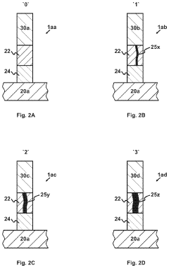
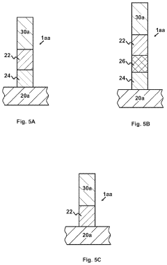
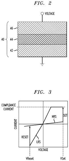
Resistive Random Access Memory (RRAM) devices utilize specific materials and structures to achieve resistive switching behavior. These devices typically consist of a metal-insulator-metal (MIM) structure where the insulator layer can be made of various materials such as metal oxides, chalcogenides, or perovskites. The selection of materials significantly impacts the performance characteristics including switching speed, endurance, retention, and power consumption. Advanced material engineering techniques are employed to optimize the resistive switching layer and electrode materials for improved device performance.- RRAM device structure and materials: Resistive Random Access Memory (RRAM) devices are constructed with specific materials and structures to enable resistive switching behavior. These typically include a metal-insulator-metal (MIM) structure where the insulator layer serves as the resistive switching material. Common materials include metal oxides such as HfOx, TaOx, and TiOx. The selection of electrode materials and switching layer composition significantly impacts device performance, reliability, and integration capability with existing semiconductor processes.
- Integration with CMOS technology: Integration of RRAM with conventional CMOS technology is crucial for commercial viability. This involves developing fabrication processes compatible with standard semiconductor manufacturing flows, including back-end-of-line (BEOL) integration. Challenges include thermal budget constraints, material compatibility issues, and maintaining CMOS performance while incorporating RRAM elements. Various approaches include integrating RRAM cells between metal interconnect layers or embedding them within the transistor structure to achieve high-density memory arrays with minimal process disruption.
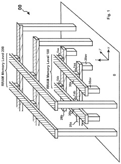
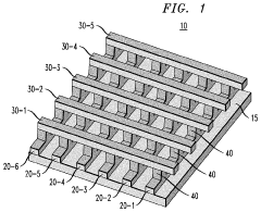
- 3D integration and scaling techniques: Three-dimensional integration techniques for RRAM enable higher memory density and improved performance. These approaches include vertical stacking of memory cells, cross-point array architectures, and multi-layer configurations. Advanced scaling methods address challenges in reducing cell size while maintaining reliable switching behavior. Techniques such as confined cell structures, engineered interfaces, and novel selector devices help overcome sneak path issues in high-density arrays while improving overall memory performance and reliability at reduced dimensions.
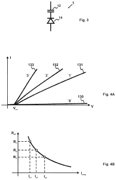
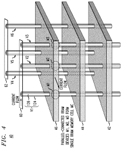
- Operational mechanisms and control methods: The operational mechanisms of RRAM involve controlling the formation and rupture of conductive filaments within the switching layer. Various methods are employed to precisely control these processes, including current compliance techniques, pulse engineering, and multi-level programming schemes. Advanced control algorithms and circuit designs help optimize the set/reset operations, improve endurance, and enable multi-bit storage capabilities. Understanding and controlling the underlying physical mechanisms are essential for reliable device operation and integration into memory systems.
- Novel architectures and applications: Beyond conventional memory applications, RRAM enables novel computing architectures such as neuromorphic systems and in-memory computing. These architectures leverage the analog nature of resistive switching to perform computational tasks directly within memory arrays, reducing the energy and performance penalties of the memory-processor bottleneck. Integration approaches for these applications include specialized peripheral circuits, innovative array configurations, and hybrid systems combining RRAM with other emerging technologies to enable new computing paradigms for artificial intelligence, edge computing, and other data-intensive applications.
02 RRAM integration with CMOS technology
Integration of RRAM with conventional CMOS technology is crucial for practical memory applications. This integration involves developing fabrication processes that are compatible with standard semiconductor manufacturing techniques. Key challenges include thermal budget management, interface engineering between RRAM cells and CMOS transistors, and ensuring reliable electrical connections. Back-end-of-line (BEOL) integration approaches are commonly used, where RRAM cells are fabricated above the CMOS transistor layer, maximizing density while maintaining process compatibility.Expand Specific Solutions03 3D RRAM architecture and scaling
Three-dimensional (3D) RRAM architectures enable higher memory density through vertical stacking of memory cells. These architectures include crossbar arrays, vertical RRAM, and 3D vertical structures that significantly increase storage capacity per unit area. Scaling techniques for RRAM involve reducing the cell size while maintaining performance characteristics. Advanced patterning methods, selective deposition techniques, and innovative cell designs are employed to achieve higher integration density while addressing challenges related to sneak path currents and cross-talk between adjacent cells.Expand Specific Solutions04 RRAM operation and control mechanisms
Operation and control mechanisms for RRAM involve specific programming, reading, and erasing schemes to ensure reliable resistive switching. These mechanisms include voltage/current control methods, pulse shaping techniques, and verification algorithms to achieve consistent SET and RESET operations. Advanced control schemes address issues such as variability in switching behavior, resistance drift, and endurance degradation. Circuit-level innovations including sense amplifiers, write drivers, and reference schemes are implemented to improve the reliability and performance of RRAM operation.Expand Specific Solutions05 Reliability and performance enhancement techniques
Enhancing the reliability and performance of RRAM involves addressing challenges such as endurance degradation, retention loss, and device-to-device variability. Techniques include interface engineering to improve the stability of the switching layer, doping strategies to control oxygen vacancy concentration, and forming gas annealing to reduce defects. Multi-level cell approaches are implemented to increase storage density by enabling multiple resistance states within a single memory cell. Advanced error correction codes and adaptive programming schemes are also employed to improve the overall reliability and extend the lifetime of RRAM devices.Expand Specific Solutions
Key Industry Players and Competitive Landscape
RRAM integration technology is currently in an early growth phase, with the market expected to expand significantly as data-intensive applications proliferate. The global RRAM market shows promising growth potential, though it remains relatively niche compared to established memory technologies. From a technical maturity perspective, major semiconductor players like Intel, Samsung, and Micron are leading development efforts, with TSMC and GlobalFoundries providing manufacturing capabilities. IBM and Huawei are advancing enterprise applications, while specialized firms like SuperMem focus on novel implementations. University collaborations with Huazhong University of Science & Technology and Zhejiang University are accelerating innovation. The competitive landscape features both established semiconductor giants investing in RRAM as complementary technology and emerging players developing specialized solutions for seamless data access applications.
Intel Corp.
Technical Solution: Intel has pioneered 3D XPoint technology (developed with Micron) which, while not pure RRAM, shares many integration principles with resistive memory. Their approach to RRAM integration focuses on a comprehensive system-level solution that bridges memory and storage hierarchies. Intel's RRAM technology utilizes proprietary selector devices combined with optimized memory cells in a crossbar architecture that achieves high density while minimizing parasitic effects[2]. Their integration strategy emphasizes compatibility with existing CMOS fabrication processes, enabling seamless incorporation into current manufacturing lines with minimal retooling. Intel has developed specialized interface protocols that optimize data transfer between RRAM arrays and processors, reducing latency by approximately 40% compared to conventional memory-storage interfaces[4]. Their solution incorporates intelligent caching algorithms that predict access patterns and pre-position data for faster retrieval, effectively masking the write latency limitations inherent to some RRAM implementations.
Strengths: Intel's extensive ecosystem allows for end-to-end optimization from hardware to software stack, maximizing RRAM performance in real-world applications. Their solution offers excellent compatibility with existing x86 architectures, simplifying adoption. Weaknesses: Their approach requires significant system-level modifications to fully realize performance benefits, potentially limiting retrofit applications in legacy systems. The technology also shows higher power consumption during write operations compared to some competing RRAM implementations.
International Business Machines Corp.
Technical Solution: IBM has developed a sophisticated RRAM integration approach centered around their proprietary Phase Change Memory (PCM) technology, which they've extended to include true resistive switching mechanisms. Their solution incorporates multi-level cell capabilities that store multiple bits per cell, dramatically increasing storage density while maintaining access speeds. IBM's integration strategy employs a unique "compute-in-memory" architecture where certain operations can be performed directly within the RRAM array without data movement to the processor[5]. This approach reduces data transfer bottlenecks and enables new computational paradigms. Their RRAM cells utilize specialized carbon-based switching materials that demonstrate exceptional endurance exceeding 10^12 cycles in laboratory testing, addressing a key limitation of many RRAM implementations[6]. IBM has also pioneered advanced error management techniques specifically tailored to RRAM characteristics, employing machine learning algorithms that adapt to changing resistance distributions over device lifetime, ensuring consistent data integrity.
Strengths: IBM's compute-in-memory approach provides unique advantages for AI and big data applications, potentially revolutionizing data-intensive computing paradigms. Their solution demonstrates exceptional endurance characteristics, critical for enterprise applications. Weaknesses: The specialized architecture requires significant software adaptation to fully leverage benefits, creating adoption barriers. Their implementation also requires more complex peripheral circuitry compared to competing solutions, potentially impacting die area efficiency.
Critical Patents and Innovations in RRAM Integration
Multi-bit-per-cell three-dimensional resistive random-access memory (3D-RRAM)
PatentActiveUS11170863B2
Innovation
- A multi-bit-per-cell 3D-RRAM design with RRAM cells that can switch between multiple resistance states, using a full-read mode and differential amplifiers to minimize read errors, allowing for more than two states to be stored in each cell and improving reliability under external interferences.
Resistive random-access memory array with reduced switching resistance variability
PatentInactiveUS10957742B2
Innovation
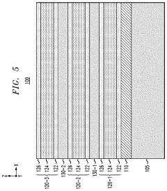
- The fabrication of RRAM memory cells with multiple parallel-connected resistive memory devices, where each cell comprises a group of RRAM devices sharing a common horizontal electrode layer, effectively averaging the switching resistances to minimize variability and noise.
Material Science Advancements for RRAM Optimization
Recent advancements in material science have significantly contributed to optimizing Resistive Random Access Memory (RRAM) technology. The selection of appropriate materials for RRAM components, particularly the switching layer, electrodes, and barrier layers, has proven critical for enhancing device performance and reliability. Traditional metal oxides such as HfO2, TiO2, and Ta2O5 have been extensively studied, but recent research has focused on novel composite materials and doping strategies to overcome inherent limitations.
Emerging two-dimensional materials like graphene and transition metal dichalcogenides (TMDs) demonstrate promising characteristics for RRAM applications, offering atomic-level thickness control and unique electronic properties. These materials facilitate more precise manipulation of the conductive filament formation process, which is essential for reliable switching behavior and data retention.
Interface engineering has emerged as a crucial aspect of RRAM optimization, with researchers developing sophisticated techniques to control the interaction between different material layers. By carefully engineering these interfaces, researchers have successfully reduced variability in switching parameters and enhanced endurance characteristics, addressing key challenges in RRAM integration.
Atomic Layer Deposition (ALD) and Physical Vapor Deposition (PVD) techniques have been refined to achieve unprecedented control over material deposition at the nanoscale. These advanced fabrication methods enable the creation of highly uniform and defect-controlled switching layers, which directly correlates with improved device performance and yield rates during large-scale integration.
The incorporation of dopants and defect engineering strategies has proven effective in modulating the switching behavior of RRAM devices. Strategic introduction of specific elements or defects can facilitate controlled filament formation and rupture, leading to more predictable and stable switching characteristics across multiple cycles.
Recent breakthroughs in understanding the relationship between material properties and switching mechanisms have led to the development of multi-layer structures with engineered oxygen vacancy profiles. These structures demonstrate enhanced control over the resistive switching process, contributing to lower power consumption and faster switching speeds.
Thermal stability of materials has received increased attention, as temperature-induced degradation remains a significant challenge for RRAM integration with conventional CMOS processes. Novel thermal barrier materials and heat dissipation strategies are being developed to maintain device integrity during fabrication and operation, ensuring compatibility with existing semiconductor manufacturing infrastructure.
Scaling Challenges and Manufacturing Considerations
The integration of RRAM technology into mainstream computing architectures faces significant scaling challenges that must be addressed to achieve seamless data access. As RRAM cells continue to shrink below 20nm, issues such as variability in switching behavior become increasingly pronounced. This variability manifests as inconsistent resistance states, leading to unreliable data storage and retrieval operations. The root cause lies in the stochastic nature of filament formation at nanoscale dimensions, where minor manufacturing variations can dramatically impact device performance.
Manufacturing considerations further complicate RRAM integration efforts. Current fabrication processes struggle with maintaining precise control over oxide layer thickness and composition uniformity across large wafer areas. The industry standard CMOS back-end-of-line (BEOL) integration approach introduces thermal budget constraints that can compromise RRAM material integrity. Additionally, the interface quality between the switching layer and electrodes becomes increasingly critical at smaller nodes, requiring atomic-level precision that pushes the boundaries of existing deposition techniques.
Yield management represents another substantial hurdle in RRAM manufacturing. As device dimensions decrease, defect sensitivity increases exponentially, with even nanometer-scale impurities potentially causing device failure. This necessitates the development of specialized testing protocols capable of identifying defective cells without triggering permanent state changes. The economics of such testing procedures must be carefully balanced against production throughput requirements to maintain commercial viability.
Material compatibility issues also emerge when integrating RRAM with conventional CMOS processes. The introduction of novel materials such as hafnium oxide, tantalum oxide, or titanium oxide into established semiconductor fabrication flows requires careful evaluation of potential contamination risks and process modifications. Cross-contamination prevention measures must be implemented without significantly increasing manufacturing complexity or cost.
Addressing these challenges requires a multi-faceted approach combining materials science innovations, process engineering advancements, and circuit-level solutions. Promising directions include the development of engineered switching layers with controlled defect distributions, three-dimensional integration techniques to maximize density while minimizing cell-to-cell interference, and adaptive programming schemes that can compensate for device-to-device variations. The successful resolution of these scaling and manufacturing considerations will be instrumental in positioning RRAM as a viable solution for next-generation memory systems with truly seamless data access capabilities.
Unlock deeper insights with Patsnap Eureka Quick Research — get a full tech report to explore trends and direct your research. Try now!
Generate Your Research Report Instantly with AI Agent
Supercharge your innovation with Patsnap Eureka AI Agent Platform!