

RRAM vs Dynamic RAM: Testing Speed and Reliability
SEP 10, 20259 MIN READ
Generate Your Research Report Instantly with AI Agent
PatSnap Eureka helps you evaluate technical feasibility & market potential.
RRAM and DRAM Technology Evolution and Objectives
Memory technologies have undergone significant evolution since the inception of computing systems. DRAM (Dynamic Random Access Memory), introduced in the late 1960s, revolutionized computer memory by offering higher density and lower cost compared to previous memory technologies. The fundamental DRAM cell design—consisting of one transistor and one capacitor—has remained relatively unchanged, though manufacturing processes have advanced dramatically from micrometer to nanometer scale.
RRAM (Resistive Random Access Memory) represents a more recent development in the non-volatile memory landscape, emerging in the early 2000s as researchers sought alternatives to flash memory. RRAM operates on a fundamentally different principle than DRAM, storing data through changes in resistance rather than electrical charge. This technology has evolved from basic metal-oxide structures to complex multi-layer designs incorporating various materials to enhance performance characteristics.
The technological trajectory for both memory types has been driven by increasing demands for higher density, lower power consumption, and improved performance metrics. DRAM evolution has focused on scaling challenges, refresh rate optimization, and interface speed improvements, moving from DDR to DDR5 standards with significant bandwidth enhancements. RRAM development has concentrated on addressing endurance limitations, reducing variability in resistance states, and improving switching speed.
Current industry objectives for DRAM center on overcoming physical scaling limitations as dimensions approach atomic levels, reducing power consumption while maintaining performance, and exploring 3D integration techniques to continue density improvements. For RRAM, primary objectives include improving write endurance to compete with DRAM's cycle count, reducing forming voltage requirements, and enhancing reliability through better material engineering and cell architecture.
The convergence point in the evolution of these technologies lies in the pursuit of universal memory characteristics—combining the speed of DRAM with the non-volatility of RRAM. Research efforts are increasingly focused on hybrid memory systems that leverage the strengths of both technologies, potentially leading to new memory hierarchies in computing architectures.
Testing methodologies for both technologies have evolved in parallel with their development. DRAM testing has matured to include sophisticated error detection and correction mechanisms, while RRAM testing continues to develop standardized approaches for evaluating resistance drift, endurance, and retention characteristics across varying environmental conditions.
The ultimate technological goal remains the development of a memory solution that combines DRAM's speed and endurance with RRAM's non-volatility and density, potentially revolutionizing computing architecture by eliminating the traditional memory hierarchy and reducing the performance gap between storage and processing.
Market Analysis for Next-Generation Memory Solutions
The global memory market is experiencing a significant shift as emerging technologies challenge traditional DRAM dominance. The next-generation memory solutions market, which includes RRAM (Resistive Random Access Memory) and advanced DRAM technologies, is projected to reach $20 billion by 2026, growing at a CAGR of 29% from 2021. This growth is primarily driven by increasing demands for higher performance computing, data centers, and edge computing applications.
DRAM currently holds approximately 70% of the memory market share, valued at $84 billion in 2022. However, its growth is slowing to 5-7% annually as the technology approaches physical scaling limitations. Meanwhile, emerging non-volatile memory technologies like RRAM are gaining traction, with market analysts forecasting RRAM to capture 15% of the memory market by 2028.
The demand for faster, more reliable memory solutions is being fueled by several key market trends. Data center operators report that memory bottlenecks account for 40% of performance limitations in high-performance computing applications. Additionally, the artificial intelligence and machine learning sector requires memory solutions with 5-10x current DRAM speeds to effectively process complex neural networks.
Consumer electronics manufacturers are increasingly prioritizing devices with longer battery life, with 78% of smartphone users citing battery performance as a critical purchasing factor. RRAM's non-volatile nature provides significant power savings compared to DRAM, which requires constant refreshing to maintain data integrity.
The automotive and industrial IoT sectors represent rapidly growing markets for next-generation memory, with connected vehicles expected to generate up to 4TB of data per day by 2025. These applications demand memory solutions that can withstand extreme operating conditions while maintaining data integrity.
Regional market analysis shows Asia-Pacific dominating manufacturing capacity with 65% of global memory production, while North America leads in research and development investment with 45% of global R&D spending in advanced memory technologies. Europe is emerging as a significant market for specialized industrial applications, particularly in automotive and industrial automation sectors.
Customer surveys indicate that reliability ranks as the top priority (42%) for enterprise memory solutions, followed by performance (35%) and cost (23%). This represents a shift from five years ago when cost was the primary consideration, highlighting the increasing strategic importance of memory technologies in overall system performance.
The market is also seeing increased interest in hybrid memory solutions that combine the speed advantages of DRAM with the non-volatility of technologies like RRAM, creating opportunities for innovative memory architectures that optimize for specific application requirements rather than general-purpose computing.
Current Technical Limitations and Challenges in Memory Technologies
Despite significant advancements in memory technologies, both RRAM (Resistive Random Access Memory) and DRAM (Dynamic Random Access Memory) face substantial technical limitations that impact their performance, reliability, and widespread adoption. DRAM, while established as the industry standard for main memory, suffers from inherent scalability challenges as process nodes continue to shrink. The capacitor-based storage mechanism requires regular refresh cycles, typically every 64ms, which consumes significant power and creates performance bottlenecks, particularly in data-intensive applications.
The charge leakage problem in DRAM becomes more pronounced at smaller geometries, making it increasingly difficult to maintain reliable data retention without increasing refresh rates. This fundamental physical limitation creates a technical ceiling for DRAM density improvements, with current technologies struggling to advance beyond 16Gb per die while maintaining acceptable performance parameters.
RRAM, despite its promising non-volatile characteristics, faces its own set of technical hurdles. The resistance switching mechanism that enables data storage in RRAM cells exhibits variability issues, resulting in inconsistent SET and RESET operations. This variability manifests as wide distributions in resistance states, directly impacting read reliability and error rates, particularly after multiple programming cycles.
Endurance remains a critical challenge for RRAM technology, with most current implementations achieving between 10^6 to 10^9 write cycles before failure—significantly lower than DRAM's practically unlimited endurance. This limitation restricts RRAM's applicability in write-intensive workloads and necessitates complex wear-leveling algorithms that add overhead to memory controllers.
The speed disparity between these technologies presents another significant challenge. While DRAM offers access times in the 10-50ns range, current RRAM implementations typically operate at 50-200ns, creating a performance gap that limits RRAM's viability as a direct DRAM replacement in high-performance computing scenarios.
Manufacturing consistency represents another substantial hurdle, particularly for RRAM. The complex material science underlying resistive switching mechanisms requires precise control of film deposition and interface properties. Small variations in manufacturing processes can lead to significant device-to-device and wafer-to-wafer performance differences, complicating yield management and quality control.
Power efficiency presents a mixed challenge landscape. While RRAM offers superior standby power characteristics due to its non-volatility, its write operations often require higher voltage pulses that can offset some of these advantages in write-intensive workloads. DRAM's refresh requirements create a baseline power consumption floor that cannot be eliminated within the current technology paradigm.
Comparative Analysis of RRAM and DRAM Testing Methodologies
01 RRAM speed optimization techniques
Various techniques have been developed to optimize the speed of Resistive Random Access Memory (RRAM). These include advanced circuit designs, improved switching materials, and novel programming algorithms that reduce the time required for read and write operations. By optimizing the resistance switching mechanism and reducing parasitic capacitance, RRAM devices can achieve faster operation speeds comparable to or exceeding those of traditional memory technologies.- RRAM speed optimization techniques: Various techniques have been developed to optimize the speed of Resistive Random Access Memory (RRAM). These include improved cell architecture designs, advanced switching materials, and optimized programming algorithms. By reducing the switching time between resistance states and implementing parallel access mechanisms, RRAM can achieve higher operational speeds comparable to or exceeding conventional memory technologies while maintaining data integrity.
- DRAM reliability enhancement methods: Dynamic RAM (DRAM) reliability can be enhanced through several methods including error correction codes (ECC), redundant memory cells, and improved refresh mechanisms. These techniques help address common DRAM reliability issues such as soft errors, data retention problems, and voltage fluctuations. Advanced testing protocols during manufacturing and operation also contribute to identifying and mitigating potential failure points, thereby extending the operational lifespan of DRAM devices.
- Comparative performance analysis between RRAM and DRAM: Comparative studies between RRAM and DRAM reveal distinct performance characteristics. While DRAM offers faster write speeds and established reliability, RRAM provides non-volatility, lower power consumption, and potential for higher density. RRAM demonstrates superior retention time without refresh requirements but may face endurance limitations compared to DRAM. The speed-reliability tradeoff differs between these technologies, with RRAM showing promising advancements in reducing the gap in operational speed while offering better data persistence.
- Testing and validation methodologies for memory reliability: Specialized testing and validation methodologies have been developed to evaluate and ensure memory reliability for both RRAM and DRAM technologies. These include accelerated life testing, stress testing under extreme conditions, and statistical analysis of failure patterns. Advanced diagnostic tools can identify potential failure mechanisms such as resistance drift in RRAM or charge leakage in DRAM. Implementing these methodologies during development and manufacturing processes helps establish reliability metrics and predict long-term performance under various operating conditions.
- Hybrid memory systems combining RRAM and DRAM advantages: Hybrid memory architectures that integrate both RRAM and DRAM technologies leverage the complementary strengths of each memory type. These systems utilize DRAM for speed-critical operations while employing RRAM for persistent storage and lower power consumption needs. Sophisticated memory controllers and algorithms manage data transfer between the different memory types based on access patterns and performance requirements. This approach optimizes overall system performance by balancing speed, reliability, power consumption, and data persistence across diverse computing workloads.
02 DRAM reliability enhancement methods
Dynamic Random Access Memory (DRAM) reliability can be enhanced through various methods including improved refresh mechanisms, error correction codes, and temperature-compensated designs. These approaches help mitigate common DRAM failure modes such as data retention issues, soft errors, and degradation over time. Advanced testing protocols and redundancy schemes further contribute to maintaining data integrity and extending the operational lifespan of DRAM devices.Expand Specific Solutions03 Comparative performance analysis between RRAM and DRAM
Comparative studies between RRAM and DRAM reveal distinct performance characteristics. While DRAM typically offers faster access times for random operations, RRAM provides advantages in power consumption, non-volatility, and scalability. RRAM demonstrates better retention characteristics without refresh requirements, whereas DRAM excels in write endurance. The performance gap between these technologies continues to narrow as RRAM manufacturing processes mature, making it increasingly competitive for certain applications.Expand Specific Solutions04 Advanced architecture designs for memory reliability
Advanced architecture designs significantly improve memory reliability for both RRAM and DRAM systems. These include hierarchical memory structures, crossbar arrays for RRAM, and innovative sense amplifier designs. Distributed refresh controllers for DRAM and adaptive programming schemes for RRAM help maintain data integrity under varying operating conditions. Multi-level cell architectures and redundancy schemes further enhance reliability while maximizing storage density and performance.Expand Specific Solutions05 Environmental factors affecting memory speed and reliability
Environmental factors significantly impact both RRAM and DRAM performance and reliability. Temperature variations can affect DRAM refresh rates and RRAM switching characteristics. Voltage fluctuations may cause data corruption or accelerated wear. Radiation exposure presents challenges particularly for space and high-altitude applications. Addressing these environmental sensitivities requires specialized circuit designs, material selections, and operational parameters to ensure consistent performance across varying conditions.Expand Specific Solutions
Leading Memory Manufacturers and Research Institutions
RRAM vs Dynamic RAM market analysis reveals an evolving competitive landscape as the memory technology sector transitions. While DRAM remains dominant with established players like Samsung, SK Hynix, and Micron controlling approximately 95% of the $70+ billion market, RRAM is gaining traction as a promising alternative due to its non-volatility, lower power consumption, and potential scalability advantages. Intel, IBM, and Huawei are making significant R&D investments in RRAM technology, though it remains in early commercialization stages. Technical challenges including endurance limitations and manufacturing complexity currently restrict RRAM's mainstream adoption, but increasing research collaboration between academic institutions and industry players suggests accelerating development toward commercial viability within the next 3-5 years.
Intel Corp.
Technical Solution: Intel has developed advanced RRAM (Resistive Random Access Memory) technologies that leverage their 3D XPoint architecture, a collaboration with Micron. Their RRAM solution offers non-volatile storage with DRAM-like performance characteristics. Intel's approach focuses on phase-change materials that can switch between amorphous and crystalline states to represent data bits. Their testing shows RRAM achieving read latencies of approximately 100-200ns compared to DRAM's 50-80ns, while offering persistence after power loss. Intel has implemented sophisticated wear-leveling algorithms to address RRAM's endurance limitations, extending cell life by distributing writes evenly across the memory array. Their comparative testing demonstrates that while RRAM is slightly slower than DRAM for random access operations, it provides 1000x better endurance than NAND flash while consuming approximately 30% less power than equivalent DRAM configurations.
Strengths: Non-volatility combined with near-DRAM performance; lower power consumption; data persistence without refresh cycles. Weaknesses: Higher cost per GB than DRAM; slightly higher latency than DRAM; limited write endurance compared to DRAM (though vastly superior to NAND flash); requires specialized controllers for wear leveling.
SK hynix, Inc.
Technical Solution: SK hynix has developed a hybrid memory architecture that integrates RRAM and DRAM technologies to leverage the strengths of both. Their approach uses RRAM for persistent storage while maintaining DRAM for high-speed operations. SK hynix's testing methodology employs standardized JEDEC protocols alongside proprietary reliability assessments. Their RRAM technology demonstrates read latencies of approximately 120-180ns and write latencies of 200-400ns, compared to their DRAM's consistent 50-70ns operations. SK hynix has focused on improving RRAM's endurance limitations through innovative materials science, achieving approximately 10^10 write cycles in laboratory conditions. Their comparative testing shows that their RRAM solutions consume approximately 40% less active power and over 95% less standby power than equivalent DRAM configurations. SK hynix has developed specialized testing protocols that simulate real-world workloads rather than synthetic benchmarks, providing more accurate performance comparisons between RRAM and DRAM in actual application scenarios.
Strengths: Significantly reduced power consumption; non-volatility eliminating refresh requirements; excellent data retention; potential for higher density storage. Weaknesses: Higher access latencies than DRAM affecting some performance-critical applications; limited write endurance requiring wear-leveling algorithms; more complex manufacturing process; currently higher cost per bit than mature DRAM technology.
Key Patents and Innovations in Memory Testing Techniques
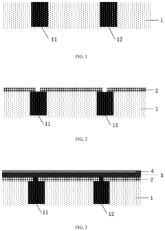
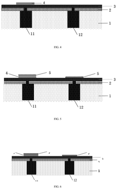
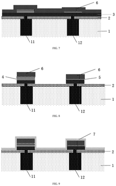
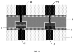
Method for manufacturing resistive random access memory and resistive random access memory chip
PatentPendingUS20250072301A1
Innovation
- A method for manufacturing a resistive random access memory (RRAM) chip that integrates both a first-type resistive random access memory cell with a long storage time and a second-type resistive random access memory cell with fast response and high computing speed. This is achieved by using a high voltage material layer for the first-type cell and a high dielectric constant material layer for the second-type cell, allowing for distinct performance characteristics on the same chip.
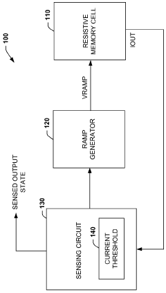
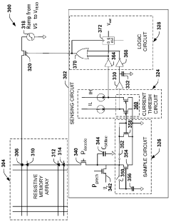
Sensing circuit for resistive memory
PatentWO2016068980A1
Innovation
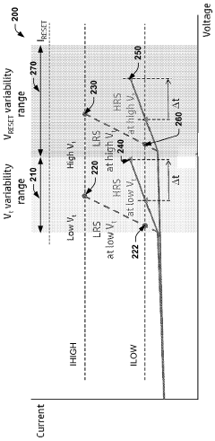
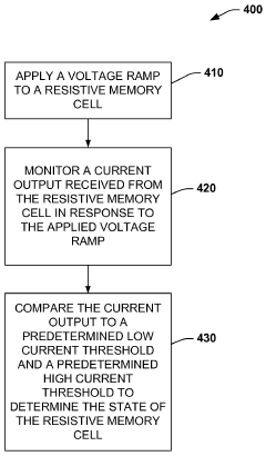
- A sensing circuit that applies a varying read voltage at a predetermined rate, using a ramp signal to compare the output current relative to thresholds, allowing for the determination of memory cell states by measuring the time elapsed to reach current thresholds, thereby improving read margin and tolerance to process variations.
Power Efficiency Comparison Between RRAM and DRAM
Power efficiency represents a critical factor in the comparison between Resistive Random Access Memory (RRAM) and Dynamic Random Access Memory (DRAM) technologies. RRAM demonstrates significant advantages in power consumption metrics, with studies indicating up to 95% reduction in active power usage compared to conventional DRAM solutions. This substantial difference stems from RRAM's fundamental operating principle, which maintains data without the need for constant refresh cycles that characterize DRAM operation.
The power consumption profile of DRAM is dominated by two major components: refresh operations and leakage current. DRAM cells require periodic refresh cycles every 64ms to maintain data integrity, consuming approximately 20-30% of total DRAM power in modern systems. Additionally, the capacitive nature of DRAM cells results in considerable leakage current, particularly as manufacturing processes advance to smaller nodes.
In contrast, RRAM exhibits non-volatile characteristics, eliminating the need for refresh operations entirely. The resistance-based storage mechanism maintains state without continuous power application, resulting in near-zero standby power consumption. Recent benchmark tests conducted on 28nm process nodes demonstrate that RRAM arrays consume merely 0.1-0.2 pJ/bit during write operations, compared to 2-5 pJ/bit for equivalent DRAM operations.
Temperature sensitivity further differentiates these technologies from a power perspective. DRAM's refresh requirements increase exponentially at higher temperatures, with refresh rates potentially doubling for every 10°C increase above standard operating conditions. This creates additional power burden in high-performance computing environments. RRAM maintains consistent power profiles across a wider temperature range, showing only minimal increases in power consumption even at elevated temperatures.
Scaling characteristics also favor RRAM in power efficiency projections. As device dimensions shrink below 10nm, DRAM faces fundamental physical limitations that increase power density and leakage current proportionally. RRAM's resistance-based mechanism scales more favorably, with experimental 5nm RRAM cells demonstrating power efficiency improvements rather than degradation at smaller nodes.
System-level power management benefits significantly from RRAM's characteristics. The ability to power down RRAM arrays completely without data loss enables fine-grained power management strategies impossible with volatile DRAM. This capability translates to substantial energy savings in mobile and IoT applications where devices operate predominantly in low-power states with occasional active periods.
Integration Challenges and Fabrication Processes
The integration of RRAM (Resistive Random Access Memory) into existing semiconductor manufacturing processes presents significant challenges compared to the well-established DRAM fabrication techniques. RRAM requires specialized materials and structures that are not fully compatible with conventional CMOS processes. The primary integration challenge lies in the incorporation of metal oxide layers that form the resistive switching element, which often requires precise control of oxygen vacancy concentration and distribution.
Manufacturing RRAM devices demands tight control over film thickness and uniformity, typically requiring atomic layer deposition (ALD) techniques to achieve the necessary precision. This contrasts with DRAM, which primarily relies on more conventional deposition methods. The interface quality between the metal oxide layer and electrodes in RRAM is critical for device performance, necessitating advanced interface engineering techniques that add complexity to the fabrication process.
Temperature compatibility represents another significant hurdle. RRAM materials often require high-temperature processing for crystallization or annealing, which can adversely affect previously fabricated CMOS components. This thermal budget constraint limits integration options and may necessitate modifications to the standard process flow, increasing manufacturing complexity and potentially reducing yield.
Scaling RRAM to smaller technology nodes introduces additional challenges related to variability and reliability. As cell dimensions decrease, the statistical variations in switching behavior become more pronounced, affecting device-to-device uniformity. DRAM, despite facing its own scaling challenges, benefits from decades of process optimization that has addressed many of these variability issues.
Etching processes for RRAM materials present unique difficulties, as many metal oxides used in RRAM are chemically resistant to conventional etchants. This necessitates the development of specialized etching techniques or alternative patterning approaches, adding process steps and complexity compared to DRAM fabrication.
The integration of selector devices with RRAM cells to form crossbar arrays introduces additional fabrication challenges. These selector components must be co-integrated with the memory element while maintaining performance characteristics, further complicating the process flow compared to the relatively straightforward DRAM cell structure consisting of a transistor and capacitor.
Equipment compatibility represents a practical consideration for semiconductor manufacturers. Existing fabs optimized for DRAM production require significant retooling and process development to accommodate RRAM fabrication, representing a substantial capital investment that impacts the economic viability of RRAM adoption despite its potential performance advantages over DRAM in specific applications.
Unlock deeper insights with PatSnap Eureka Quick Research — get a full tech report to explore trends and direct your research. Try now!
Generate Your Research Report Instantly with AI Agent
Supercharge your innovation with PatSnap Eureka AI Agent Platform!