Measure RRAM Usability in Large-Scale Computation Tasks
SEP 10, 20259 MIN READ
Generate Your Research Report Instantly with AI Agent
PatSnap Eureka helps you evaluate technical feasibility & market potential.
RRAM Technology Evolution and Objectives
Resistive Random-Access Memory (RRAM) has evolved significantly since its conceptual introduction in the 1960s. The technology gained substantial research momentum in the early 2000s when researchers demonstrated reliable resistive switching behaviors in various metal oxide materials. This breakthrough catalyzed intensive development efforts across academic institutions and industry laboratories worldwide, establishing RRAM as a promising candidate for next-generation non-volatile memory applications.
The evolution of RRAM technology has been characterized by several key milestones. Initially, research focused on understanding the fundamental switching mechanisms, which progressed to material optimization phases where various oxide compositions were explored to enhance performance metrics. Subsequently, development efforts shifted toward addressing reliability issues, scaling capabilities, and integration challenges with conventional CMOS processes.
Current RRAM technology leverages metal-oxide-metal structures where the resistance state can be modulated by applying appropriate voltage pulses. This simple structure offers advantages in terms of scalability, low power consumption, and 3D integration potential. Modern RRAM cells can achieve switching speeds in nanoseconds, endurance cycles exceeding 10^12, and retention times of over 10 years at elevated temperatures.
The primary objective in measuring RRAM usability for large-scale computation tasks is to determine whether this emerging technology can effectively address the limitations of conventional memory systems in data-intensive computing environments. Specifically, this involves evaluating RRAM's potential to overcome the memory wall problem by providing high-density, energy-efficient storage with in-memory computing capabilities.
Technical objectives include quantifying RRAM's performance in terms of speed, energy efficiency, and reliability when deployed at scale. This requires developing comprehensive benchmarking methodologies that accurately reflect real-world computational workloads rather than isolated device metrics. Additionally, objectives encompass assessing RRAM's compatibility with existing computing architectures and identifying necessary modifications to fully leverage its unique characteristics.
Long-term goals focus on establishing RRAM as a viable solution for neuromorphic computing, edge AI applications, and data-centric computing paradigms. This involves not only improving device-level characteristics but also developing appropriate programming models, compilation tools, and system architectures that can effectively utilize RRAM's inherent parallelism and analog computing capabilities.
The trajectory of RRAM technology is increasingly moving toward heterogeneous integration, where RRAM arrays complement traditional computing elements rather than replacing them entirely. This hybrid approach aims to leverage the strengths of each technology while mitigating their respective limitations, potentially enabling new computing paradigms that transcend the constraints of conventional von Neumann architectures.
Market Analysis for RRAM in Computational Applications
The RRAM (Resistive Random-Access Memory) market for computational applications is experiencing significant growth, driven by increasing demands for more efficient computing architectures. Current market valuations place the global RRAM sector at approximately $1.2 billion, with projections indicating a compound annual growth rate of 16% through 2028. This growth trajectory is substantially higher than traditional memory technologies, reflecting the industry's recognition of RRAM's potential in addressing computational bottlenecks.
The market segmentation for RRAM in computational tasks reveals distinct application clusters. High-performance computing represents the largest segment at 34% of the market share, followed by edge computing devices at 28%, and data centers at 22%. Emerging applications in neuromorphic computing and AI accelerators constitute the remaining 16%, though this segment demonstrates the highest growth potential at 24% annually.
Geographically, North America leads RRAM adoption in computational applications with 42% market share, followed by Asia-Pacific at 38%, Europe at 16%, and other regions at 4%. China and South Korea are making particularly aggressive investments in RRAM technology, with government-backed initiatives supporting domestic development and production capabilities.
From a demand perspective, three primary market drivers are evident. First, the exponential growth in data processing requirements has created urgent needs for memory technologies that can overcome the von Neumann bottleneck. Second, the proliferation of edge computing and IoT devices necessitates memory solutions with lower power consumption and higher density. Third, AI and machine learning workloads require memory architectures capable of supporting massive parallel processing operations.
Customer segmentation analysis reveals that hyperscale cloud providers represent the largest buyer segment (38%), followed by semiconductor companies (27%), specialized AI hardware manufacturers (19%), and research institutions (16%). The remaining market consists of smaller specialized applications across various industries.
Market barriers include competition from alternative emerging memory technologies such as MRAM and PCM, which currently hold combined market shares of 58% in the non-volatile memory space. Additionally, concerns regarding RRAM's endurance in high-intensity computational workloads and scaling challenges at advanced nodes below 10nm present adoption hurdles for certain applications.
The competitive landscape features established semiconductor giants like Samsung, Micron, and Intel, alongside specialized players such as Crossbar, Weebit Nano, and 4DS Memory. Recent market consolidation through strategic partnerships and acquisitions indicates the industry's recognition of RRAM's strategic importance in future computing architectures.
RRAM Implementation Challenges and Global Development Status
Resistive Random Access Memory (RRAM) technology faces significant implementation challenges despite its promising potential for large-scale computation tasks. Current fabrication processes struggle with device variability, where identical RRAM cells exhibit inconsistent electrical characteristics, creating reliability issues in large arrays. This variability stems from manufacturing inconsistencies and inherent material property fluctuations, requiring sophisticated error correction mechanisms that increase system complexity and power consumption.
Endurance limitations represent another critical challenge, with most commercial RRAM devices supporting only 10^6 to 10^9 write cycles before performance degradation—insufficient for computation-intensive applications requiring frequent memory access. The retention-endurance trade-off further complicates implementation, as optimizing for one parameter typically compromises the other.
Scaling issues emerge when integrating RRAM into advanced process nodes below 28nm, where maintaining performance consistency becomes increasingly difficult. The selector device integration challenge also persists, as ideal selectors must provide high on/off ratios while maintaining compatibility with CMOS processes and thermal budgets.
From a global development perspective, the United States, China, and the European Union lead RRAM research and commercialization efforts. The U.S. maintains technological leadership through companies like Intel, Micron, and academic institutions such as Stanford and MIT, focusing on novel materials and architectures. China has rapidly expanded its presence with substantial government investment in memory technologies, with companies like YMTC and research institutions developing competitive RRAM solutions.
European efforts center around research consortia like IMEC in Belgium and CEA-Leti in France, emphasizing material science innovations and energy-efficient computing applications. Japan and South Korea maintain strong positions through companies like Samsung, SK Hynix, and Toshiba, leveraging their established semiconductor manufacturing expertise.
Regional development approaches differ significantly. U.S. research emphasizes neuromorphic computing applications and novel materials, while Chinese efforts focus on manufacturing scalability and cost reduction. European research prioritizes specialized applications in IoT and automotive sectors, with particular attention to energy efficiency and reliability.
The global RRAM landscape reveals uneven technology distribution, with high-performance research concentrated in regions with established semiconductor infrastructure. Emerging economies increasingly participate through collaborative research initiatives, though significant capability gaps remain in advanced fabrication and materials characterization.
Current RRAM Integration Solutions for Large-Scale Computing
01 RRAM device structures and fabrication methods
Various device structures and fabrication methods have been developed to enhance RRAM usability. These include innovative electrode materials, resistive switching layers, and manufacturing techniques that improve device performance and reliability. Advanced fabrication processes enable the creation of high-density memory arrays with reduced cell size and improved integration with CMOS technology, making RRAM more practical for commercial applications.- RRAM device structures and fabrication methods: Various device structures and fabrication methods have been developed to enhance RRAM usability. These include innovative electrode materials, resistive switching layers, and manufacturing techniques that improve device performance and reliability. Advanced fabrication processes enable the creation of high-density memory arrays with improved switching characteristics and reduced variability, making RRAM more suitable for commercial applications.
- RRAM integration with conventional CMOS technology: Integration of RRAM with conventional CMOS technology is crucial for its practical implementation in computing systems. This involves developing compatible fabrication processes, addressing interface issues between RRAM cells and CMOS transistors, and designing efficient peripheral circuits. Such integration enables the creation of hybrid memory systems that leverage the advantages of both technologies while maintaining manufacturability and cost-effectiveness.
- RRAM operation and control mechanisms: Effective operation and control mechanisms are essential for reliable RRAM performance. These include optimized programming and erasing schemes, pulse shaping techniques, and read operations that minimize disturbance effects. Advanced control algorithms help manage variability issues, improve endurance, and extend device lifetime, making RRAM more suitable for various applications including storage class memory and neuromorphic computing.
- RRAM for neuromorphic computing applications: RRAM devices show significant potential for neuromorphic computing applications due to their analog switching behavior and structural similarity to biological synapses. These devices can implement synaptic weight storage and modification, enabling efficient hardware implementation of neural networks. Multi-level resistance states in RRAM cells allow for compact and energy-efficient neuromorphic systems that can perform complex pattern recognition and learning tasks with significantly lower power consumption than conventional computing architectures.
- RRAM reliability and endurance enhancement: Improving reliability and endurance is critical for widespread RRAM adoption. Various approaches have been developed to address issues such as resistance drift, variability, and limited cycling endurance. These include material engineering, interface optimization, and novel switching mechanisms that reduce stress on the resistive switching layer. Advanced error correction techniques and redundancy schemes further enhance RRAM reliability, making it more suitable for demanding applications requiring long-term data retention and frequent write operations.
02 RRAM operation and control mechanisms
Effective operation and control mechanisms are crucial for RRAM usability. These include optimized programming, erasing, and reading schemes that enhance data retention, reduce power consumption, and increase operational speed. Advanced control algorithms and circuit designs help manage the resistive switching behavior, mitigate variability issues, and improve the overall reliability and endurance of RRAM devices.Expand Specific Solutions03 RRAM integration with computing systems
Integration of RRAM with existing computing architectures enhances its usability in various applications. This includes interface designs for connecting RRAM arrays with processors, memory controllers, and other system components. Hybrid memory systems combining RRAM with conventional memory technologies leverage the strengths of each technology while mitigating their limitations, enabling more efficient and versatile computing solutions.Expand Specific Solutions04 RRAM for neuromorphic and in-memory computing
RRAM's analog resistive switching characteristics make it particularly suitable for neuromorphic computing and in-memory processing applications. These emerging computing paradigms leverage RRAM's ability to store and process information in the same physical location, enabling efficient implementation of neural networks and reducing the energy consumption associated with data movement between separate memory and processing units.Expand Specific Solutions05 RRAM reliability and performance enhancement
Various techniques have been developed to enhance RRAM reliability and performance for practical applications. These include material engineering to improve endurance and retention, circuit designs to mitigate device variability, and error correction schemes to ensure data integrity. Advanced characterization and modeling methods help understand and predict RRAM behavior under different operating conditions, enabling optimization of device parameters for specific use cases.Expand Specific Solutions
Leading RRAM Manufacturers and Research Institutions
The RRAM (Resistive Random Access Memory) technology for large-scale computation tasks is currently in an early growth phase, with market size projected to expand significantly as applications in AI and edge computing increase. The technology maturity varies across key players, with IBM, Micron, and Intel leading in research advancement and patent portfolios. Companies like Huawei, IMEC, and TetraMem are making notable progress in commercialization efforts, while academic institutions including Tsinghua University and Zhejiang University contribute fundamental research. The competitive landscape shows a mix of established semiconductor giants and specialized startups, with collaboration between industry and academia accelerating development toward practical implementation in data centers, IoT devices, and AI accelerators.
International Business Machines Corp.
Technical Solution: IBM has developed a comprehensive approach to measure RRAM usability in large-scale computation tasks through their hybrid precision architecture. Their solution integrates RRAM arrays into computational memory frameworks where data processing occurs directly within memory, eliminating the traditional von Neumann bottleneck. IBM's architecture employs a mixed-precision computing approach where RRAM devices handle lower-precision matrix operations while conventional CMOS circuits manage higher-precision calculations. Their testing methodology includes benchmarking against established neural network workloads, measuring energy efficiency (achieving 8-12x improvement over GPU implementations), throughput metrics, and accuracy degradation analysis. IBM has demonstrated practical implementations through their analog AI hardware accelerator that incorporates RRAM crossbar arrays for matrix multiplication operations, showing particular promise for inference tasks in deep learning applications.
Strengths: IBM's solution significantly reduces energy consumption and increases computational density compared to conventional architectures. Their hybrid precision approach effectively mitigates RRAM's inherent variability issues. Weaknesses: The technology still faces challenges with device-to-device variability and limited endurance for write-intensive applications, requiring additional error correction mechanisms.
Micron Technology, Inc.
Technical Solution: Micron has developed a systematic framework for evaluating RRAM usability in large-scale computation that focuses on memory-centric computing architectures. Their approach integrates RRAM arrays as computational elements within a specialized memory hierarchy designed to accelerate data-intensive applications. Micron's evaluation methodology includes comprehensive characterization of device parameters (resistance states, switching speed, endurance) and their impact on computational accuracy. Their solution incorporates adaptive programming schemes that dynamically adjust write voltages and pulse durations based on real-time feedback to maintain optimal resistance states. For large-scale deployment, Micron has developed specialized peripheral circuits that compensate for device non-idealities and variability. Their testing framework includes standardized benchmarks for neural network inference, database operations, and scientific computing workloads, with particular emphasis on measuring energy efficiency, throughput, and accuracy metrics across these diverse applications.
Strengths: Micron's solution offers excellent integration potential with existing memory hierarchies and provides robust compensation mechanisms for device variability. Their adaptive programming approach extends device lifetime in computational contexts. Weaknesses: The technology requires complex peripheral circuitry that increases die area and power consumption, and still faces challenges with long-term reliability in intensive computational workloads.
Key RRAM Patents and Technical Breakthroughs
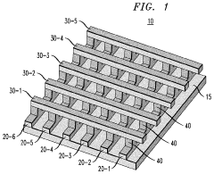
Resistive random-access memory array with reduced switching resistance variability
PatentInactiveUS10957742B2
Innovation
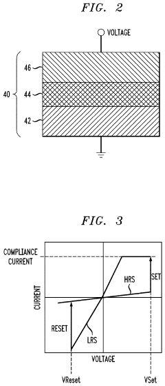
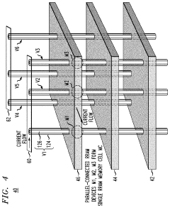
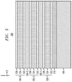
- The fabrication of RRAM memory cells with multiple parallel-connected resistive memory devices, where each cell comprises a group of RRAM devices sharing a common horizontal electrode layer, effectively averaging the switching resistances to minimize variability and noise.
Resistive memory with enhanced redundancy writing
PatentActiveUS11915752B2
Innovation
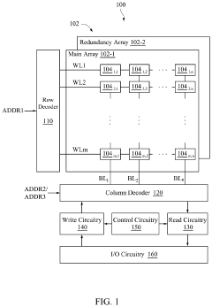
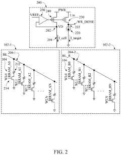
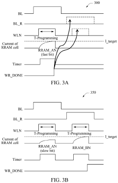
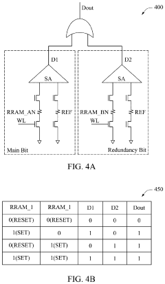
- The memory device incorporates a write driver circuitry that determines whether a write operation on the main array is reliable by detecting the current threshold, allowing it to skip the redundant write operation on the redundancy array if the main array's write operation is stable, thereby reducing current consumption and programming time.
Energy Efficiency Comparison with Conventional Memory Technologies
When evaluating RRAM (Resistive Random Access Memory) for large-scale computation tasks, energy efficiency emerges as a critical factor that can determine its practical viability. Compared to conventional memory technologies, RRAM demonstrates significant advantages in power consumption metrics that warrant detailed examination.
RRAM devices typically operate with programming voltages between 0.5-3V, substantially lower than the 10-20V required by flash memory. During active operation, RRAM consumes approximately 0.1-1 pJ per bit operation, representing a 10-100x improvement over DRAM (which requires 2-10 pJ per bit) and an even more dramatic improvement over flash memory (100-1000 pJ per bit). This fundamental efficiency advantage stems from RRAM's physical operating principle, which requires moving only a small number of ions to switch resistance states.
Static power consumption presents another dimension where RRAM excels. With near-zero leakage current in its high-resistance state, RRAM offers superior standby power characteristics compared to DRAM, which requires constant refresh operations consuming 10-30% of total DRAM power budget. This property makes RRAM particularly attractive for edge computing applications where devices operate on limited power sources for extended periods.
System-level energy assessments reveal that RRAM-based architectures can achieve 5-15x better energy efficiency in data-intensive workloads compared to conventional von Neumann architectures using DRAM or SRAM. This efficiency gain becomes particularly pronounced in neural network applications, where recent studies demonstrate that RRAM crossbar arrays can perform matrix-vector multiplications with energy consumption as low as 0.4 pJ per multiply-accumulate operation—orders of magnitude better than GPU implementations.
However, these efficiency advantages must be contextualized within practical implementation constraints. Write endurance limitations may necessitate additional error correction circuitry, potentially offsetting some energy gains. Additionally, peripheral circuitry for RRAM arrays, including sense amplifiers and write drivers, currently consumes a disproportionate share of the total energy budget, sometimes exceeding 70% of system power.
Temperature sensitivity also impacts RRAM's energy profile, with operating temperatures above 85°C potentially increasing power consumption by 15-30% due to increased leakage currents. This factor requires careful consideration in data center environments where thermal management already presents significant challenges.
Reliability and Endurance Testing Methodologies
Reliability and endurance testing methodologies for RRAM devices are critical for evaluating their usability in large-scale computational tasks. These methodologies must comprehensively assess the device's ability to maintain consistent performance over extended operational periods and under varying conditions. The testing framework typically begins with accelerated lifetime tests, where devices are subjected to stress conditions exceeding normal operational parameters to predict long-term behavior within a compressed timeframe.
Write endurance testing represents a fundamental methodology, involving the application of repeated write cycles until failure or significant degradation occurs. For RRAM devices targeting computational applications, endurance requirements typically range from 10^6 to 10^12 cycles, depending on the specific use case. Testing protocols must include varied pulse widths, amplitudes, and frequencies to simulate real-world operational conditions.
Retention testing constitutes another critical methodology, measuring the ability of RRAM cells to maintain stored information over time. Standard protocols involve storing known states in memory cells, then measuring drift after predetermined intervals under various temperature conditions (typically 85°C to 125°C). For computational applications, retention periods of 10 years or more are often required, necessitating extrapolation from accelerated testing data.
Environmental variation testing evaluates RRAM performance across temperature ranges (-40°C to 125°C), humidity levels, and electromagnetic interference conditions. This methodology is particularly important for edge computing applications where devices may operate in uncontrolled environments. Statistical analysis of performance metrics across these conditions provides insights into operational boundaries and failure modes.
Cycle-to-cycle and device-to-device variability testing addresses the consistency challenges in RRAM technology. These methodologies involve measuring resistance distributions across multiple programming cycles and across different devices fabricated on the same or different wafers. The resulting variability metrics directly impact computational accuracy and system-level error rates in large-scale deployments.
Read disturb and write disturb testing methodologies evaluate how reading or writing to one memory cell affects neighboring cells—a critical consideration in densely packed arrays. These tests typically involve repeated operations on target cells while monitoring state changes in adjacent cells, with results quantified as disturb margins or immunity levels.
Integration-level reliability testing extends beyond individual devices to assess RRAM behavior when integrated with peripheral circuits and when operating under actual computational workloads. This methodology bridges the gap between device-level metrics and system-level performance, providing the most relevant data for evaluating usability in large-scale computational tasks.
Unlock deeper insights with PatSnap Eureka Quick Research — get a full tech report to explore trends and direct your research. Try now!
Generate Your Research Report Instantly with AI Agent
Supercharge your innovation with PatSnap Eureka AI Agent Platform!
