

Measure RRAM Memory Size on Data Processing Capabilities
SEP 10, 20259 MIN READ
Generate Your Research Report Instantly with AI Agent
PatSnap Eureka helps you evaluate technical feasibility & market potential.
RRAM Technology Background and Objectives
Resistive Random Access Memory (RRAM) has emerged as a promising non-volatile memory technology over the past two decades, offering significant advantages in terms of power consumption, scalability, and integration capabilities compared to traditional memory technologies. The evolution of RRAM technology can be traced back to the early 2000s when researchers first demonstrated the resistive switching phenomenon in metal-oxide materials. Since then, RRAM has progressed from laboratory experiments to commercial prototypes, with major semiconductor companies investing heavily in its development.
The fundamental operating principle of RRAM relies on the formation and rupture of conductive filaments within a dielectric material, allowing for binary or multi-level data storage. This mechanism enables RRAM to achieve high density, fast switching speeds, and excellent endurance characteristics. Recent technological advancements have further improved RRAM's performance metrics, making it increasingly viable for various applications including edge computing, Internet of Things (IoT) devices, and neuromorphic computing systems.
Current RRAM technology trends indicate a shift towards three-dimensional architectures, multi-bit storage capabilities, and enhanced reliability through novel materials and fabrication techniques. The integration of RRAM with CMOS technology has also gained significant momentum, enabling hybrid memory-logic systems that can overcome the von Neumann bottleneck in conventional computing architectures. This integration capability positions RRAM as a key enabler for in-memory computing paradigms.
The primary objective of measuring RRAM memory size on data processing capabilities is to establish a quantitative relationship between memory capacity and computational performance in RRAM-based systems. This relationship is crucial for optimizing system designs for specific applications, particularly those requiring efficient data processing at the edge. Understanding this correlation will enable more effective resource allocation and system scaling strategies for future RRAM implementations.
Another key objective is to determine the optimal memory size for different data processing workloads, considering factors such as energy efficiency, processing speed, and area constraints. This optimization is particularly important for resource-constrained environments where maximizing computational capability per unit of memory is essential. The findings from such measurements will guide the development of application-specific RRAM architectures that balance memory resources with processing requirements.
Furthermore, this research aims to explore the unique characteristics of RRAM that differentiate it from conventional memory technologies in terms of data processing capabilities. These include its inherent parallelism, analog computing potential, and in-situ processing abilities. Quantifying these advantages will provide valuable insights for system designers and accelerate the adoption of RRAM in next-generation computing platforms.
Market Demand Analysis for RRAM Memory Solutions
The global market for RRAM (Resistive Random Access Memory) solutions is experiencing significant growth driven by increasing demands for high-performance, energy-efficient memory technologies across multiple sectors. Current market projections indicate that the RRAM market is expected to grow at a compound annual growth rate of 16% through 2028, with the total addressable market reaching approximately $4 billion by that time.
The primary market demand for RRAM memory solutions stems from data-intensive applications that require rapid processing capabilities. Edge computing applications represent one of the fastest-growing segments, with enterprises seeking memory solutions that can process data locally to reduce latency and bandwidth usage. This segment is projected to grow by 22% annually as IoT deployments accelerate across industrial and consumer sectors.
Artificial intelligence and machine learning applications constitute another significant market driver. The need for memory architectures that can efficiently handle neural network operations has created substantial demand for RRAM solutions that offer parallel processing capabilities. Market research indicates that AI hardware acceleration represents a $1.2 billion opportunity for RRAM technologies by 2026.
Enterprise data centers are increasingly exploring RRAM solutions to address the growing gap between processing speeds and memory access times. With data processing requirements doubling approximately every two years, traditional memory hierarchies are becoming bottlenecks in system performance. RRAM's ability to serve as both storage and computing element positions it as a promising solution for in-memory computing architectures.
Consumer electronics manufacturers are showing heightened interest in RRAM for next-generation mobile devices and wearables. The market demand is driven by requirements for lower power consumption while maintaining high performance. Battery-powered devices benefit significantly from RRAM's non-volatile nature and low operating power, with potential energy savings of up to 60% compared to conventional memory technologies.
Automotive applications represent an emerging market segment with stringent requirements for memory reliability and performance under extreme conditions. Advanced driver-assistance systems and autonomous vehicles require memory solutions that can process sensor data in real-time while withstanding harsh environmental conditions. This segment is expected to grow at 19% annually through 2027.
Geographic analysis reveals that North America currently leads RRAM market demand with 38% market share, followed by Asia-Pacific at 35% and Europe at 22%. However, the Asia-Pacific region is expected to show the highest growth rate over the next five years due to increasing semiconductor manufacturing capacity and rising adoption of advanced electronics in countries like China, South Korea, and Taiwan.
RRAM Technical Challenges and Development Status
Resistive Random Access Memory (RRAM) technology has emerged as a promising candidate for next-generation non-volatile memory solutions due to its high density, low power consumption, and compatibility with CMOS processes. However, several significant technical challenges currently impede its widespread commercial adoption and limit its data processing capabilities relative to memory size.
The scaling limitations present a primary challenge for RRAM development. While theoretically capable of scaling below 10nm, practical implementations face issues with variability and reliability at these dimensions. This variability manifests as inconsistent switching behavior, with cycle-to-cycle and device-to-device variations becoming more pronounced as cell size decreases, directly impacting the effective memory capacity that can be reliably utilized for data processing tasks.
Endurance constraints further complicate RRAM implementation in data-intensive applications. Current RRAM cells typically achieve 10^6 to 10^9 write cycles before failure, which falls short of DRAM (10^15 cycles) and even some competing non-volatile memories. This limitation creates a direct correlation between memory size and processing capability, as larger arrays are needed to implement wear-leveling techniques that distribute write operations across the memory array.
Retention characteristics pose another significant challenge, with data retention times varying from years to mere hours depending on operating conditions and material systems. This variability necessitates complex refresh schemes that consume additional power and processing resources, reducing the effective data processing throughput per unit of memory.
The sneak path current problem in crossbar architectures represents a fundamental obstacle to increasing array sizes. As array dimensions grow, parasitic currents through unselected cells create read disturbances and increase power consumption. Various selector devices and architectural solutions have been proposed, but each introduces additional complexity and potential points of failure.
From a manufacturing perspective, RRAM faces integration challenges with standard CMOS processes. While theoretically compatible, the introduction of new materials and the requirement for precise control of oxide layer formation create yield issues that impact cost-effectiveness at larger memory sizes.
The global research landscape shows concentrated efforts in addressing these challenges, with significant contributions from research institutions in the United States, China, South Korea, and Europe. Industry players like Intel, Samsung, and emerging startups are actively developing solutions to overcome these limitations, with recent advancements in material engineering and array architecture showing promising results for improving the relationship between memory size and data processing capabilities.
Current RRAM Memory Sizing Methodologies
01 Scaling and miniaturization of RRAM cells
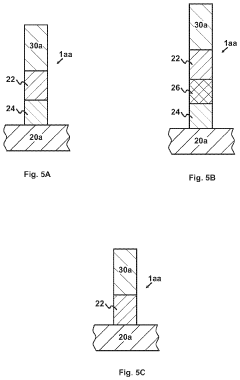
RRAM technology enables significant scaling down of memory cell size compared to conventional memory technologies. Various approaches focus on reducing the physical dimensions of RRAM cells to achieve higher density memory arrays. These include innovative electrode designs, optimized switching materials, and advanced fabrication techniques that allow for sub-nanometer feature sizes while maintaining reliable resistive switching properties.- Scaling and miniaturization of RRAM cells: RRAM technology enables significant scaling down of memory cell size compared to conventional memory technologies. Various approaches focus on miniaturizing RRAM cells to achieve higher density storage while maintaining performance. These approaches include innovative electrode designs, novel materials for switching layers, and advanced fabrication techniques that allow for sub-nanometer feature sizes. Miniaturization efforts aim to achieve memory cells in the nanometer range while addressing challenges related to reliability and endurance at smaller dimensions.
- 3D architecture for increased memory capacity: Three-dimensional integration of RRAM cells enables significant increases in memory density without expanding the footprint of the memory array. By stacking memory cells vertically, 3D RRAM architectures can achieve much higher storage capacities compared to planar configurations. These architectures include vertical RRAM arrays, cross-point structures, and multi-layer integration approaches. The 3D integration addresses the physical limitations of two-dimensional scaling while maximizing storage capacity within a given area.
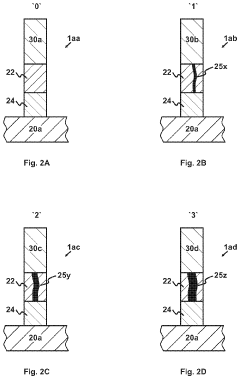
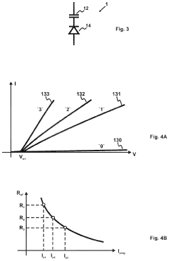
- Multi-level cell technology for increased storage density: Multi-level cell (MLC) technology in RRAM allows each memory cell to store multiple bits of information rather than just binary states. By precisely controlling the resistance states of the memory cell, MLC RRAM can achieve multiple distinguishable resistance levels, effectively multiplying the storage capacity without increasing the physical number of cells. This approach requires sophisticated programming algorithms and sensing circuits to reliably distinguish between the different resistance states while maintaining data integrity over time.
- Novel materials and structures for optimized RRAM size: Advanced materials and innovative structural designs are being developed to optimize RRAM cell size and performance. These include metal oxides with enhanced switching properties, two-dimensional materials, and specialized electrode configurations. Novel selector devices and integration schemes help reduce cell-to-cell interference in high-density arrays. These material innovations enable smaller cell sizes while addressing challenges related to power consumption, endurance, and retention time in scaled-down RRAM devices.
- System-level integration and memory size optimization: System-level approaches focus on optimizing the overall memory size and efficiency of RRAM implementations. These include innovative memory array architectures, peripheral circuitry designs, and system integration techniques that maximize effective storage capacity. Advanced addressing schemes, error correction methods, and data compression techniques further enhance the effective memory size. System-level optimizations also consider the balance between memory density, access speed, power consumption, and reliability to meet specific application requirements.
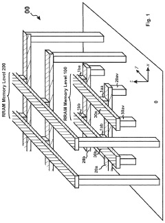
02 3D stacking and vertical integration for increased memory capacity
Three-dimensional stacking architectures are employed to increase RRAM memory capacity without expanding the horizontal footprint. By vertically stacking multiple layers of RRAM cells, the effective memory density can be significantly increased. These 3D architectures include vertical RRAM arrays, cross-point structures, and multi-layer integration schemes that maximize storage capacity while minimizing chip area.Expand Specific Solutions03 Multi-level cell (MLC) technology for increased bit density
Multi-level cell technology in RRAM allows storing multiple bits of information in a single memory cell by utilizing different resistance states. By precisely controlling the resistance levels, RRAM cells can achieve 2, 3, or even 4 bits per cell, effectively multiplying the memory capacity without increasing the physical cell count. This approach requires sophisticated programming algorithms and sensing circuits to reliably distinguish between the multiple resistance states.Expand Specific Solutions04 Novel materials and structures for high-density RRAM
Advanced materials and innovative structural designs are being developed to enhance RRAM memory density. These include oxide-based switching materials, two-dimensional materials, and nanoscale filamentary structures that enable reliable switching at extremely small dimensions. By optimizing the material composition and structure, these approaches achieve higher memory density while maintaining good retention, endurance, and switching characteristics.Expand Specific Solutions05 System-level integration and memory array architecture
System-level integration techniques and optimized memory array architectures are crucial for maximizing effective RRAM memory size. These include innovative addressing schemes, efficient peripheral circuitry, and optimized array configurations that reduce overhead and increase usable memory capacity. Advanced controller designs and error correction techniques also help maintain data integrity at higher densities, effectively increasing the practical memory size that can be achieved with RRAM technology.Expand Specific Solutions
Key RRAM Industry Players and Ecosystem
The RRAM memory size measurement landscape is evolving rapidly, with the market currently in its growth phase. The global RRAM market is expanding at a CAGR of approximately 30%, driven by increasing data processing demands. Leading players include Samsung Electronics and Micron Technology, who are investing heavily in RRAM technology development. Companies like GLOBALFOUNDRIES and TSMC are advancing manufacturing processes, while Huawei and Intel are exploring RRAM integration in their systems. Research institutions such as Zhejiang Lab and Nanjing University of Posts & Telecommunications are collaborating with industry partners to overcome technical challenges. The technology is approaching maturity, with Samsung, Micron, and Macronix demonstrating viable prototypes, though widespread commercial deployment remains limited as optimization for data processing applications continues.
Samsung Electronics Co., Ltd.
Technical Solution: Samsung has developed advanced RRAM solutions focused on optimizing memory size for enhanced data processing capabilities. Their approach implements a vertically stacked 3D RRAM architecture that significantly increases memory density while maintaining fast access times. Samsung's technology utilizes a unique cell structure with engineered switching materials that demonstrate improved retention and endurance characteristics. Their solution incorporates intelligent memory controllers that dynamically allocate memory resources based on workload requirements, optimizing the balance between capacity and performance. Samsung has developed specialized peripheral circuits that support in-memory computing operations, allowing certain data processing tasks to be performed directly within the memory array. Their RRAM technology implements multi-level cell capabilities, storing multiple bits per cell to effectively increase memory density without expanding the physical footprint. Samsung has also developed comprehensive testing methodologies to accurately measure how different RRAM memory configurations impact various data processing workloads.
Strengths: Industry-leading manufacturing capabilities ensure high yield and reliability; vertical integration allows optimization across memory and processing components; extensive experience with memory technologies enables rapid innovation. Weaknesses: Higher power consumption during write operations compared to some competing technologies; complex manufacturing process increases production costs; requires specialized software optimization to fully leverage capabilities.
Hewlett Packard Enterprise Development LP
Technical Solution: HPE has pioneered memristor-based RRAM technology through their Memory-Driven Computing architecture. Their approach focuses on measuring RRAM memory size impact on data processing through a novel crosspoint architecture that enables massive parallelism. HPE's memristor technology implements a unique non-volatile memory fabric where memory cells are arranged in a dense crossbar configuration, allowing for efficient scaling to large array sizes while maintaining performance characteristics. Their solution incorporates specialized sensing circuits that can accurately detect multi-level resistance states, effectively increasing the bit density per cell. HPE has developed custom algorithms that dynamically adjust the memory allocation based on workload requirements, optimizing the balance between memory size and processing capabilities. Their architecture supports direct in-memory computing operations, enabling certain computations to be performed within the memory array itself rather than transferring data to a separate processor.
Strengths: Revolutionary memory-centric architecture eliminates traditional memory-processor bottlenecks; superior energy efficiency for data-intensive applications; scalable design supports future capacity expansion. Weaknesses: Relatively new technology with less field validation than established memory types; requires significant software ecosystem adaptation; higher initial implementation costs compared to conventional memory solutions.
Core RRAM Scaling and Performance Metrics
Multi-bit-per-cell three-dimensional resistive random-access memory (3D-RRAM)
PatentActiveUS11170863B2
Innovation
- A multi-bit-per-cell 3D-RRAM design with RRAM cells that can switch between multiple resistance states, using a full-read mode and differential amplifiers to minimize read errors, allowing for more than two states to be stored in each cell and improving reliability under external interferences.
Resistive random-access memory devices
PatentActiveUS9378785B2
Innovation
- The implementation of a write-back mechanism in RRAM devices, involving a memory array, read circuit, write-back circuit, and write-back logic circuit, which changes the resistance state of selected memory cells from a low to a high resistance state after reading, preventing current leakage and maintaining data integrity.


RRAM Integration with Computing Architectures
The integration of RRAM with computing architectures represents a pivotal advancement in addressing the memory wall challenge that has long constrained computational efficiency. Traditional von Neumann architectures suffer from the bottleneck created by separate processing and memory units, resulting in significant data transfer overhead. RRAM offers a compelling solution through its ability to be seamlessly integrated into various computing paradigms.
In-memory computing architectures leveraging RRAM demonstrate remarkable advantages for data-intensive applications. By performing computational operations directly within the memory array, these architectures eliminate the need for constant data movement between separate processing and storage units. The crossbar structure of RRAM arrays naturally supports matrix operations, making them particularly efficient for neural network implementations where weight matrices must be rapidly accessed and processed.
Neuromorphic computing systems benefit substantially from RRAM integration due to the device's inherent characteristics that mimic biological synaptic behavior. The analog conductance states of RRAM cells can represent synaptic weights, while their non-volatile nature enables persistent storage of learned patterns. This biological resemblance facilitates more efficient implementation of neural algorithms compared to traditional digital approaches.
Edge computing platforms increasingly incorporate RRAM to enable sophisticated data processing capabilities in resource-constrained environments. The low power consumption and non-volatility of RRAM allow edge devices to perform complex computations while maintaining extended battery life. This integration is particularly valuable for IoT applications where real-time data processing must occur with minimal energy expenditure.
Hybrid computing architectures combining RRAM with conventional CMOS technology represent a pragmatic approach to leveraging RRAM's benefits while maintaining compatibility with existing systems. These architectures typically employ RRAM for specific memory-intensive tasks while utilizing traditional processors for control functions and operations less suited to RRAM implementation.
The memory size of RRAM arrays directly impacts their data processing capabilities across these architectural integrations. Larger arrays enable more complex operations to be performed in parallel but introduce challenges related to sneak path currents and voltage drops. Conversely, smaller arrays offer better control but limit computational capacity. Finding the optimal balance between array size and operational efficiency remains a critical consideration when designing RRAM-based computing systems.
Energy Efficiency Considerations for RRAM Systems
Energy efficiency has emerged as a critical factor in the development and deployment of RRAM (Resistive Random Access Memory) systems, particularly when evaluating memory size requirements for data processing applications. RRAM's inherent characteristics offer significant advantages in power consumption compared to conventional memory technologies, with typical operating power ranging from 10-100 μW during active states and less than 1 μW in standby mode.
The relationship between RRAM memory size and energy efficiency follows a non-linear pattern. Smaller memory arrays generally demonstrate better energy efficiency per bit operation, but this advantage diminishes as array sizes increase due to parasitic capacitances and resistance in interconnect structures. Research indicates that optimally sized RRAM arrays (typically 128×128 to 256×256 cells) achieve the best balance between energy consumption and data processing capabilities.
Peripheral circuitry contributes significantly to the overall energy profile of RRAM systems. Sense amplifiers, write drivers, and address decoders can account for 30-45% of total system power consumption. Advanced designs implementing low-swing voltage techniques and adaptive power management have demonstrated energy reductions of up to 60% in these components without compromising performance.
The energy cost of data movement between RRAM arrays and processing units represents another critical consideration. Recent architectures implementing in-memory computing paradigms have shown promising results by reducing data movement energy by 70-85% compared to conventional von Neumann architectures. This approach becomes increasingly beneficial as memory size scales up, particularly for data-intensive applications like neural network inference.
Temperature sensitivity also impacts RRAM energy efficiency, with operating temperatures above 85°C potentially increasing leakage current by 2-3× and reducing retention time. Advanced thermal management techniques and adaptive refresh schemes have been developed to mitigate these effects, maintaining energy efficiency across broader temperature ranges.
Multi-level cell (MLC) RRAM configurations offer increased storage density but introduce energy efficiency trade-offs. While MLC designs can double or quadruple effective memory capacity within the same physical footprint, they typically require 30-50% more energy per bit operation due to more complex read/write circuits and error correction mechanisms. This relationship must be carefully considered when sizing RRAM systems for specific data processing workloads.
Unlock deeper insights with PatSnap Eureka Quick Research — get a full tech report to explore trends and direct your research. Try now!
Generate Your Research Report Instantly with AI Agent
Supercharge your innovation with PatSnap Eureka AI Agent Platform!